Lupine Publishers Group
Lupine Publishers
Menu
ISSN: 2641-6921
Review Article(ISSN: 2641-6921) 
Materials Driving Survivability, Radiation Hardening, and Shielding of Integrated Circuits in a Radiation Environment Volume 4 - Issue 1
Jacek Karpiesiuk*
- Expert in Construction and Building Specialties, Bialystok University of Technology, Poland
Received: March 18, 2021; Published: March 31, 2021
*Corresponding author: Bahman Zohuri, Adjunct Professor, Business Analytics School, Golden Gate University, Ageno School of Business, San Francisco, California
DOI: 10.32474/MAMS.2021.04.000177
Abstract
With recent renewal interest in survivability, radiation hardening against cold or hot x-ray as well as high power laser energy among defense companies and military communities, radiation shielding of military equipment becomes an imperative task and requirement. Materials used in radiation shielding is one way to go to protect any vulnerable digital circuits in form of an integrated circuit, and consequently selecting of such ICs for a radiation environment also becomes a necessity as part of survivability requirements. Thermomechanical properties of materials as part of shielding are also going to play a huge role as part of protection of these ICs as well. With most countries getting involved with their nuclear arsenal development, protection of our assets in space or on ground such as electric circuits and grids is another issue that we need to think about to survive a nuclear burst both Endo and Exo-atmospheric circumstance. The effects of nuclear explosions produce both immediate and delayed destructive effects, that requires choice of right and proper protective materials for ICs to be shielded and survivable in such radiation environment driven by a nuclear weapon burst. Nuclear weapon effects in term of blast, thermal radiation, electromagnetic pulse, and prompt ionizing radiation, etc. are part of concerns for choosing the proper materials. Radiation shielding is based on the principle of attenuation, which is the ability to reduce a waves or ray’s effect by blocking or bouncing particles through a barrier material. This short review is discussing different holistic issues in respect to selected materials and integrated circuits in respect to survivability and shielding within a radiation environment, either man-made or natural.
Keywords: Integrated circuits; digital circuits; radiation shielding; electromagnetic pulse; electromagnetic interference; electromagnetic compatibility
Introduction
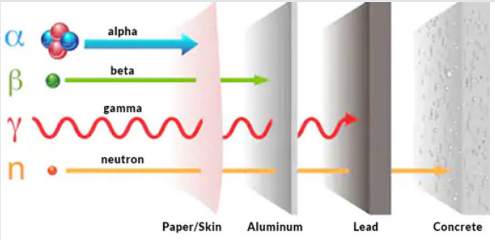
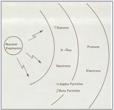
To start with, we introduce the basic concept of radiation by
describing what it is and then we move on to introduce types of
shielding materials that we need to protect our assets, as well as
going through different radiation types of radiation as illustrated
in (Figure 1), that we need to shield ourselves, biologically, health
care wise and medical imaging to the yields from nuclear energy
burst, nuclear medicine and non- destructive testing cross different
industries and on earth and in the space as well as ground assets
within defense communities. As illustrated in (Figure 1) to X-Ray
radiation both cold and hot X-Ray radiation as well has High Energy
Laser (HEL) radiation. We then talk about different source of
radiation either man-made or natural ones that one need to shield
against it no matter what field of application we are considering.
Under effort of As Low as Reasonable (ALARA) driving a principle
that strives to minimize the exposure of ionizing radiation to
people and environment by choosing and introducing the proper
materials, while considering economics, technology, and social
factors. Considering all the factors, and the number of materials to
choose from, consulting with a shielding materials expert within
such community of experts in the field of radiation shielding and
survivability, is essential to finding the most effective solutions to
your shielding needs.
It all starts with the type of radiation that is present. Materials
interact differently with different types of radiation. For example,
tungsten can attenuate gamma radiation effectively, but when
exposed to neutron radiation, secondary gamma rays can be produced. Materials that are strongest at attenuation gamma
radiation are tungsten and lead, while high density concrete and
borated polyethylene are better materials for stopping neutrons on
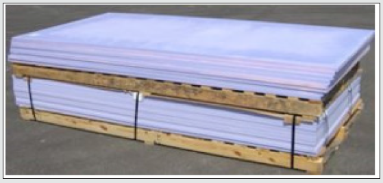
its track. (Figure 2) is illustration of such materials. Choosing the
right material will allow you to save space and use less material.
A shield of high-density concrete can take half the space of
regular concrete with the same shielding properties. Flexibility of
a material is also important to think about when considering the
space requirements. A flexible material like metal impregnated
polymers might be more suitable to shield a round object like a
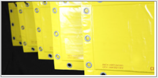
pipe, as it can be wrapped around tightly as (Figure 3), shows such
wrapping materials.
Materials that are used in radiation shielding, are consistent
of certain physical and chemical properties that would be able
to enhance shielding to level of assigned survivability of certain
Service Level Agreement (SLA), depending on the environmental
conditions that need to take place. Radiation shielding is imperative
as radiation can be a serious concern in nuclear power facilities,
industrial or medical x-ray systems, radioisotope projects, particle
accelerator work, and several other circumstances. Containing
radiation and preventing it from causing physical harm to
employees or their surroundings is an important part of operating
equipment that emits potentially hazardous rays. Preserving both
human safety and structural material that may be compromised
from radiation exposure are vital concerns, as well as shielding
sensitive materials, such as electronic devices and photographic
film. From military application perspective, any Integrated
Circuits (ICs) that are embedded in any electronic devices as
part of military equipment’s need to be radiation harden in case
of directed exposure to X-Ray radiation either cold or hot as well
type of particle radiation type shown in (Figure 1), here resulted
from any nuclear explosion either Endo or Exo-atmospheric burst.
Integrated Circuits these days are digital rather than analog if form
of old tubes technology that we could find in any electronic devices
such as old Radios representing Transistor, Capacitors or Resistors.
Digital circuits are designed and manufactured in Semiconductor’s
industries in form of either Bipolar or CMOS infrastructures.
However, most of these industries are pushing CMOS approach
that is heavily driven by reduction of chip’s footprint on these
day’s 25” wafer processing, toward sub-micron technology path.
Although from survivability, point of view the Bipolar IC’s have a
better chance than CMOS circuits to not to have any latch-up events
due to Transient Radiation Effects on Electronics (TREE) from a
Single Event Upset (SEU) or System Generated Electromagnetic
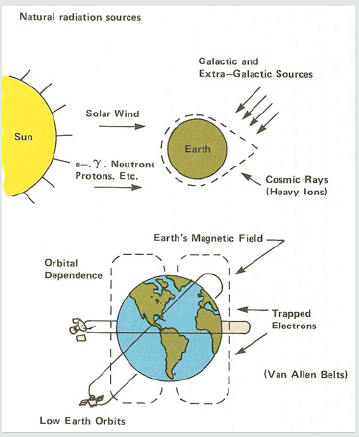
Pulse (SGEMP) [1]. All these above events could take place either
naturally as a source or man-made type such as nuclear explosion,
where the intensity of radiation depending on the yield of weapons
in question as illustrated in (Figures 4 & 5). Environments with
large amount of ionizing radiation, either natural or man-made,
create special design challenges for integrated circuits, typically for
RF power amplifier chips [2]. A single charged particle can knock
thousands of electrons loose, resulting in electronic noise and signal
spikes. In the case of digital circuits, this can lead to results that
are inaccurate or unintelligible. It is a particularly serious problem
in designing artificial satellites, spacecraft, military aircraft, nuclear
power stations and nuclear weapons. The process of regulating the
effects and degree of penetration of radioactive rays varies according
to the type of radiation involved. Indirectly ionizing radiation,
which includes neutrons, gamma rays, and x-rays, is categorized
separately from directly ionizing radiation, which involves charged
particles. Different radiation shielding materials are better suited
for certain types of radiation than others, as determined by the interaction
between specific particles and the elemental properties of
the shielding material. Moreover, in the case of digital circuits, this
can lead to results that are inaccurate or unintelligible. It is a particularly
serious problem in designing artificial satellites, spacecraft,
military aircraft, nuclear power stations and nuclear weapons. Typical
sources of exposure of electronics to ionizing radiation are the
Van Allen radiation belts for satellites, nuclear reactors in power
plants for sensors and control circuits, residual radiation from isotopes
in chip packaging materials, cosmic radiation for spacecraft
and high-altitude aircraft and nuclear explosions for potentially all
military and civilian electronics [3].
As part of protecting the ICs or any other assets against radiation threat is the shielding and packaging materials. Is the way to go, as it was stated in above. When it comes to protecting against radiation, the basic radiation protection principals or radiation safety tips involve time, distance, and shielding. Time, in this case, means to limit exposure to the minimum amount possible. Distance means staying as far from radiation sources as possible as a best practice. The intensity of radiation generally follows the inverse square law, meaning that it falls off with the square of the distance from the source. Moving twice the distance away from a source of radiation reduces the intensity of exposure by a factor of 1/22 or one fourth the value. Beyond time and distance, making use of effective shielding is the other approach to managing exposure to radiation. But what materials protect against radiation? The most common ones used include lead, concrete, and water - or a combination of these. Below
X-Ray and Gamma Radiation Shielding Materials
In most common cases, radiation such as X-Ray or Gamm- Radiation source, either natural or man-made, high density-density materials with high atomic number Z are more effective than lowdensity with atomic number Z alternatively has a better shielding effect for blocking or reducing the intensity of radiation. However, low-density materials can compensate for the disparity with increased thickness, which is as significant as density in shielding applications. Lead is particularly well-suited for lessening the effect of gamma rays and X-Rays due to its high atomic number. This number refers to the number of protons within an atom, so a lead atom has a relatively high number of protons along with a corresponding number of electrons. These electrons block many of the gamma and x-ray particles that try to pass through a lead barrier, and the degree of protection can be compounded with thicker shielding barriers. However, it is important to remember that there is still potential for some rays making it through shielding and that an absolute barrier may not be possible in many situations [4].
Alpha and Beta Shielding
In most cases, high-density materials are more effective than low-density alternatives for blocking or reducing the intensity of radiation. However, low-density materials can compensate for the disparity with increased thickness, which is as significant as density in shielding applications. Lead is particularly well-suited for lessening the effect of gamma rays and x-rays due to its high atomic number. This number refers to the number of protons within an atom, so a lead atom has a relatively high number of protons along with a corresponding number of electrons. These electrons block many of the gamma and x-ray particles that try to pass through a lead barrier, and the degree of protection can be compounded with thicker shielding barriers. However, it is important to remember that there is still potential for some rays making it through shielding and that an absolute barrier may not be possible in many situations [4].
Neutron Shielding
Material such as Lead is quite ineffective for blocking neutron
radiation, as neutrons are uncharged and can simply pass-through
dense materials. Materials composed of low atomic number
elements are preferable for stopping this type of radiation because
they have a higher probability of forming cross-sections that will
interact with the neutrons. Hydrogen and hydrogen-based materials
are well-suited for this task. Compounds with a high concentration
of hydrogen atoms, such as water, form efficient neutron barriers
in addition to being relatively inexpensive shielding substances.
However, low-density materials can emit gamma rays when blocking neutrons, meaning that neutron radiation shielding is most
effective when it incorporates both high and low atomic number
elements. The low-density material can disperse the neutrons
through elastic scattering, while the high-density segments block
the subsequent gamma rays with inelastic scattering [4]. Because
neutron radiation presents so many inherent dangers, top-of-theline
neutron shielding protection is critical. Neutrons have neither
a positive nor a negative charge, resulting in a wide range of energy
and mass levels that must be blocked. Neutron radiation dangers,
therefore, must be handled with the utmost care and attention
to detail, whether dealing with nuclear power facilities, medical
X-ray systems, radioisotope projects, or particle accelerator
work. Hazardous rays can cause serious and long-lasting physical
harm to the people exposed to them, and structural material and
environments can also be damaged beyond repair by radioactive
waves. Electronic devices and photographic film are a couple of the
more sensitive mediums that can be easily damaged [5].
Given that lead is a heavy element or high atomic number Z
(heavier than around 80% or so of the other elements found on the
periodic table), it is a common choice for use in fabricating radiation
shielding products. Lead is fabricated into different product forms
to provide radiation shielding and protection, and which includes
these types:
a. Lead Sheets, Plates, Slabs, & Foils
b. Lead Shot
c. Lead Wools
d. Lead Epoxies
e. Lead Putties
f. Lead Bricks
g. Lead Pipe
h. Lead-clad Tubing
i. Lead-clad Pipe
j. Lead Sleeves
k. Lead Glass
l. Lead-Polyethylene-Boron Composites
Lead can also be added to concrete or cinder blocks for use
in wall construction. By adding unperforated sheets of lead to the
blocks and extending the sheet beyond the edge of the concrete
block and overlapping shield of lead can be embedded in a wall to
form an effective radiation barrier utilizing a continuous lining of
lead sheet. A similar approach can be used to create lead shielded
doors and door frames. As with the wall construction, it is important
to overlap the lead that is used in the door frame with the lead that
is used in the wall construction to provide a continuous lead barrier
that will function as an effective shield. There is other source of
event that is driven by man-made nuclear explosion that we need to
protect both biological and integrated circuits from and few, which
can be named are Electromagnetic Pulse (EMP), Electromagnetic
Interference (EMI) that are driven by the yield from a nuclear
explosion with Endo or Exo-Atmospheric burst. An EMP that is
resulting from above-atmosphere level detonation of a nuclear
device produces enough radiation to wreak havoc with electrical
systems. The blast produces a very brief but intense electromagnetic
field that can quickly induce very high currents in electrical devices,
shorting them out. The stronger the electromagnetic field — the
“pulse” the stronger the current, and the more likely electrical
devices are to “blow out.” It’s akin to a power surge that shorts out
your refrigerator or TV when too much voltage surges through the
electrical outlet… on a whole other scale.
Any digital integrated circuit built in any electronic device
requires to have a capability in order to be compatible to function
in such environment or to be Electromagnetic Compatible (EMC).
It is very obvious, when transition from analog circuit such as
old tube moved into path of digital circuits and consequently
manufacturing of transistor and eventually, Integrated Circuits
(ICs) in form of semiconductor, the combination of package of
sequence of events such as EMP and EMI driving a need for EMC for
the ICs becomes a necessity for shielding such as electronic devices.
These semiconductor devices, however, are more susceptible to the
effects of radiation than the old tubes and have to be made more
survivable or obey the requirement for EMC.
The survivability of these semiconductor devices is combination
of both an innovative design and shielding procedure. Packaging of
these semiconductor ICs within a layer of combined materials such
as Gallium (Ga)/Arsenide (As) provides a better protection layer
against the concerned radiation by design and Gallium Arsenide
Next Generation Semiconductors Market Expected to Grow to $22
Billion by 2026. As illustrated in (Figure 6), Next generation GaAs
semiconductors promise to bring a huge market, not totally replacing
the existing semiconductor market, but ultimately making a huge
dent in it. The ability to replace silicon semiconductors, a market
that is $500 billion dollars in 2020 makes one sit up and take notice.
The existing silicon semiconductor market is a pretty good size for
a market that barely existed in 1975. Next generation GaAs support
the signal speed that is needed to implement 5G. GaAs works in a
way that silicon cannot. The potential for the next generation GaAs
wafers is staggering, with the overall semiconductor market likely
to surpass $20 trillion by 2026 as the new industrial revolution
takes hold and 5G supports IoT that connects all things together.
Once economies of scale are realized these semiconductor GaAs
markets are expected to really take off. The sheer size of the global
semiconductor market at $500 billion dollars in 2020 shows that
the potential for next generation semiconductor technology is
truly exciting. The IC’s built-in wafer of GA/As and packaged with
these two combined materials are the best way shielding against
any natura or man-made radiation and they better opportunity of
survivability over-time.
The gallium arsenide wafers are next generation technology because they operate faster than the silicon semiconductors, they support a new, faster network called 5G. Gallium arsenide GaAs represents the next generation of semiconductor chips because the chips can do things that the silicon chips cannot do. GaAs does have a considerably higher bandgap than silicon. It is a direct bandgap semiconductor with a zinc blende crystal structure. Sensing for autonomous and electric vehicles is one use of technology. 3D Sensing for consumer electronics and use for lasers is common. Units are used in radar and lasers. The benefits of using GaAs in devices derive in part from the characteristic that GaAs generates less noise than most other types of semiconductor components. As a result, it is useful in weak-signal amplification applications. Due to these benefits related to generating less noise, GaAs is a suitable replacement for silicon in the manufacture of linear and digital ICs. A gallium arsenide wafer is also known as the Gallium arsenide substrate.
Conclusion
With the development of astronautic techniques, the radiation effects on Integrated Circuits (ICs) have been recognized by people. Environments with high levels of ionizing radiation create special design challenges for ICs. To ensure the proper operation of such systems, manufacturers of integrated circuits and sensors intended for the military aerospace markets adopt various methods of radiation hardening. The environmental conditions that the shielding is placed in is also important to consider. How well a material can withstand heat, if the shielding will be moved and potentially bumped and if the material must hold any structural load are all important factors in the environment that need to be considered. Shielding properties can change when put under stress or heated. Dents and damage to the material may also lessen the ability for a material to shield properly [6]. Safety is important in selecting the right shielding solutions. Leaded glass for example comes in several options including safety glass. Clear Leaded Acrylic is also a viable option to making durable clear shielding that is shatter resistant. Exposed lead may not be permitted in some scenarios due to the toxicity of lead, so polymers mixed with bismuth, tungsten or iron may be a better, non-toxic alternative [6]. Cost is an important to consider when selecting the appropriate shielding material for a job. Lead is a very effective and inexpensive shielding material compared to materials like tungsten and could work just as well for a lot of scenarios. Related to cost, another factor that needs to be considered is the ease of shipping, handling, and installation. Choosing between installing leaded drywall or sheet lead is one example where shipping and installation need to be considered [6].
References
- Higgins DF, Lee K, Marin L (1978) System-generated EMP. IEEE Trans. Electromagnetic Compatibility 20: 14-22.
- Barbara NV, Schrimpf RD, Kerwin WJ (1990) Ionizing-radiation-induced degradation in electronic power amplifiers. Proceedings of the Conference Record of the 1990 IEEE Industry Applications Society Annual Meeting pp. 1667-1672.
- Holmes-Siedle AG, Adams L (2002) Handbook of Radiation Effects. Oxford University Press, England, UK.
- Materials Used in Radiation Shielding. II Thomas.
- The Dangers of Neutron Radiation, Frontier Technology Corporation.
- Paul Rochus ‘Choosing the Right Radiation Shielding: Factors Considered by a Shielding Materials Expert’. Marshield.

Top Editors
-

Mark E Smith
Bio chemistry
University of Texas Medical Branch, USA -

Lawrence A Presley
Department of Criminal Justice
Liberty University, USA -

Thomas W Miller
Department of Psychiatry
University of Kentucky, USA -

Gjumrakch Aliev
Department of Medicine
Gally International Biomedical Research & Consulting LLC, USA -

Christopher Bryant
Department of Urbanisation and Agricultural
Montreal university, USA -

Robert William Frare
Oral & Maxillofacial Pathology
New York University, USA -

Rudolph Modesto Navari
Gastroenterology and Hepatology
University of Alabama, UK -

Andrew Hague
Department of Medicine
Universities of Bradford, UK -

George Gregory Buttigieg
Maltese College of Obstetrics and Gynaecology, Europe -

Chen-Hsiung Yeh
Oncology
Circulogene Theranostics, England -
.png)
Emilio Bucio-Carrillo
Radiation Chemistry
National University of Mexico, USA -
.jpg)
Casey J Grenier
Analytical Chemistry
Wentworth Institute of Technology, USA -
Hany Atalah
Minimally Invasive Surgery
Mercer University school of Medicine, USA -

Abu-Hussein Muhamad
Pediatric Dentistry
University of Athens , Greece

The annual scholar awards from Lupine Publishers honor a selected number Read More...


