


Lupine Publishers Group
Lupine Publishers
ISSN: 2643-6744
Review ArticleOpen Access
Silicon Substrate for RF –CMOS Applications Volume 2 - Issue 2
Received: December 01, 2021; Published: December 16, 2021
*Corresponding author:Kamaljeet Singh, UR Rao Satellite Centre, Old Airport Road, Bangalore India
DOI: 10.32474/CTCSA.2021.02.000132
Abstract
Dielectric substrate selection plays important role at RF frequencies due to confinement of energy and its impact on the overall loss. The substrate permittivity which correlates with the energy storage significantly affects the circuit performance at higher frequencies. The substrates are segregated into lossy dielectric or good dielectric according to the permittivity behavior. The loss tangent value depends on the permittivity and affects the quality factor of the transmission line. In silicon the metal contact give rise to the Schottky contact due to metal- semiconductor junction. This necessitates proper formulation and modeling to be carried out for predicting circuit behavior. Various phenomena such as doping, carrier mobility, frequency is the major contributing factor effecting the permittivity and their role on loss tangent are studied and detailed in this article.
Keywords: Substrate; Complex Permittivity; Silicon; Resistivity
Introduction
Silicon with finite resistivity behaves differently at RF frequencies compared to generic substrate considered as a good dielectric such as alumina, RT-Duroid, FR4. Lossy as well as good dielectric material can be characterized by complex permittivity. Silicon which is considered as the lossy substrate also have considerable amount of dissipative energy associated with the complex permittivity. Permittivity is the property of the dielectric which indicates capacitance or stored charges mathematically associated with the imaginary part. The loss tangent can be deduced with the current density which in turn depends on complex permittivity. Material permittivity relates with the physical phenomena and main contributors are ionic conduction, dipole friction, and dipolar relaxation, atomic and electronic polarization [1]. Real part of the complex permittivity remains constant up to microwaves but reduces at millimeter wave region whereas imaginary part increases in this region and it can be attributed to dipole relaxation whereas in infrared region the atomic and electronic polarization causes the absorption peaks resulting in more losses at higher frequencies. The effects are more prominent by the applied electric field as nucleus displace with respect to surrounding electrons in the case of electric polarization whereas in case of atomic polarization positive and negative segregation for ions higher permittivity materials particularly at higher frequencies.
Silicon as semiconductor is considered as a lossy substrate due to its finite resistivity [2]. The effect of lossy substrate on circuit performance is unpredictable and leads to higher losses leading to dissipative current [3]. This effect is primarily due to the higher bounded charges and reflects in the higher imaginary part of the permittivity which increases with the frequency. The micro strip configuration with metal- semiconductor leads to Schottky junction and the transmission line model to be modified due to this phenomenon. This necessitates proper modeling of the silicon substrate for predicting the behavior at RF frequencies [4]. Transmission line on silicon behaves as diode rather than pure conductive line and commonly employed planar transmission line is micro strip [5,6]. Micro strip structure consists of the metalized top and bottom surface in which silicon acts as a dielectric layer between two conducting surfaces. The behavior of silicon varies as it consists of both free and bounded charges which varies with frequency. Further metal contact with the semi-conductor leads to Schottky behavior and having conduction as well as displacement current density. The resistivity of silicon can be further changed with the doping which is standard microelectronics process [7]. This necessitates modeling to predict behavior due to the various phenomena associated with the variable capacitance and resistance. The article details various factor impacting RF losses and permittivity in the silicon particularly due to resistivity, interfacial layer stacking, and frequency and discusses the associated phenomena.
Complex Permittivity
Permittivity is related with the charge retention capacity of the medium so higher dielectric constant εr generally leads to more heat. In dielectric materials with the application of external bias the bound charges are displaced which creates dipole field that opposes the applied electric filed E causing polarization of the atoms or molecules of the material [5]. Relation between displacement flux D, electric field E and polarization P can be represented as
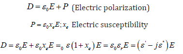
The relative permittivity can be expressed as
In case of semiconductor, charges are free and bounded which contributes the current by applying electric field. The concept of permittivity can be deduced from the Maxwell’s equation

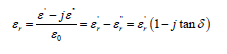
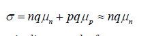
The imaginary part associated with the permittivity accounts for losses in the medium due to damping of the vibrating dipole moment [7,8]. Dielectric loss due to damping effect can be further correlated with electric susceptibility and higher susceptibility renders more heating. In the case of semiconductor σ = qμn so for frequency ‘f’ using eq (1)

The generalized conductivity can be represented as
In case of microstrip line mostly for narrow lines [9], the relative permittivity can be represented as

where c is the velocity of light, Ca is air capacitance, Cd is the dielectric capacitance. Variation of tanδ with frequency is more prominent compared to εr at microwave ranges. Lossy dielectric such as silicon having higher dielectric susceptibility leads to more polarization. The losses in the dielectric can be represented by generic term of power factor which represents power factor of condenser containing the dielectric


Table 1: Classification of dielectric material in terms of permittivity.

Concept Of Loss Tangent
Substrate permittivity affects the conductor, dielectric, and radiation loss in the microstrip line. All these mechanisms are dependent on the substrate permittivity resulting in various phenomena such as surface wave, ground wave, leaky wave or radiated wave. Selection of dielectric is very important as substrate with high dielectric constant can introduce losses. It also governs the width, propagation characteristics, line length, losses, and various modes of propagation. Generally dielectric loss is less compared to conductor losses in microwave region, but for lossy substrate such as silicon the effect is considerably high and affects the circuit performance considerably at higher frequencies. Dielectric loss represented by the loss angle (eq 1) can also be represented as:

In general case the term tan δL is negligible and only contributing factor is from tan δd . The first term tan δd resulted from the polarization loss associated with intrinsic substrate and second term tan δL is defined as extrinsic loss resulted from the finite conductivity of the substrate which is applicable for silicon [3]. Various other factors such as temperature and humidity also impact the dielectric constant value. The dielectric loss (for narrow lines) can also be represented as [11].

Dielectric loss due to damping effect can be further correlated with electric susceptibility as higher susceptibility renders more heating. Various factors effecting the dielectric loss tangent are detailed as below:
Effect of Frequency
The increase in the frequency results in the increased losses in semi-conductor compared to alumina substrate as ε ' remains constant but ε " varies with frequency, so variation in tanδ is observed as shown in Table 2. Other substrates such as TFG also demonstrate the above-mentioned effect [12].
Table 2: Frequency effect on the dielectric loss.

Effect of Impurity
In case of alumina substrate, tanδ value varies with purity level and highest purity (99.5%) yields lowest loss tangent. The increase in purity from 96% to 99.5% can change the loss tangent by 3 times. This also relates with the doping concentration as increase in impurity level increases loss tangent (Table 3).
Table 3: Impurity effect on dielectric loss.

Effect of Resistivity
Table 4: Substrate resistivity effect on dielectric loss.

The semiconductor substrate silicon also shows loss behavior varied with the change in resistivity. Table 4 shows that an order of increase in resistivity decreases the losses [13]. The above relation clearly shows that resistivity plays important role in the dielectric loss and can be correlated with the recombination time τ as

where Id is the stored charge current and is the recombination lifetime. High permittivity substrates are good at holding charges where low permittivity material having low ability to polarization and holding charges Substrate losses for silicon in case of 10k Ω -c-m are 0.032 dB/cm which increases to 32 dB/cm for the resistivity of 10 ohm-cm. High resistivity silicon substrate (1 k Ω -cm) is having attenuation of the order of 10^-3 compared to 10^-4 for silicon with resistivity of 10 k Ω -cm. The cut off frequency phenomena can be written as

Free charge carriers cause the main part of the losses in the semiconductor and as seen from equation (3), the main loss contribution is due to finite conductivity. At lower end of the frequency, real permittivity remains constant and the cut off frequency is dependent on the substrate resistivity. In semiconductor, the doping phenomena to be correlated with the change in resistivity and losses further increases as doping reduces the carrier mobility.
Transmission Line Modelling
The metal on the semiconductor material silicon results in the Schottky junction [7]. Schottky diode is having both resistance and capacitance non-linearity. The semiconductor with Schottky barrier contact can be represented as capacitance and un-depleted region as resistor. The resulting equivalent circuit is the combination of non-linear capacitance and resistance. The resistance value also varies at higher frequencies as the current through the nondepleted region can crowd to the outside edge of the material due to the skin effect [14] and thus increasing the resistance.
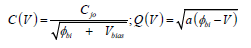
where jo C is the capacitance at zero bias voltage, a is constant and V is the applied voltage. The stored charges can be represented as: Q(V)=a0+a1V+a2V2+a3V3+…. And I (t)= dQ/dt= [ a1+2a2V+3a3V2+….] (dV/dt); where V=V0 sinωt . The equivalent model of microstrip on silicon can be shown in the (Figure 1a). The conductance G and variable capacitance (C) is accounted due to Schottky contact. The total current density in the non-depleted region can be shown as in (Figure 1b). The change in depletion layer width with the doping changes the current density. Further increase in frequency results in charge deposition which can change the resistance value in the un-depleted region [15]. The resultant phenomena shown in Table 5 summarizing the effect of various parameters on the various device aspects. Time varying electric filed induces conduction and displacement current. Polarization dipoles having finite mass moves back and forth with the frequency resulting in the delayed response and at higher frequencies, polarization vector lags behind the applied electric field. The relaxation time representing charge density decay can be represented as
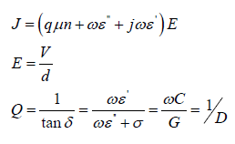
Figure 1A: Microstrip transmission line for Silicon accounted due to Schottky contact. The total current density in the nondepleted region can be shown as in Figure 1b.

Figure 1B: Conductance & capacitance due to Schottky.

Table 5: Effect of various parameters on the device.

The change in depletion layer width with the doping changes the current density. Further increase in frequency results in charge deposition which can change the resistance value in the un-depleted region [15]. The resultant phenomena shown in Table 5 summarizing the effect of various parameters on the various device aspects. Time varying electric filed induces conduction and displacement current. Polarization dipoles having finite mass moves back and forth with the frequency resulting in the delayed response and at higher frequencies, polarization vector lags behind the applied electric field. The relaxation time representing charge density decay can be represented as

The delay changes with the resistivity and at higher resistivity the delay reduce as per the equation. An order increase in the resistivity decreases approximately an order in the relaxation time. This delay is important for the charge depletion effect in the substrate and Table 6 shows delay associated with some common semiconductor materials. Permittivity value is also affected with the temperature and humidity as the mobility of charge carriers decreases with the temperature due to lattice scattering. The effect of temperature on the permittivity is shown in Table 7. Silicon substrate is deposited with the thin layer of oxide before initiating further processing [16]. So, for silicon substrate, the losses are primarily from substrate and interface losses induced between the insulation layer and silicon substrate. These losses can be minimized by employing high quality gate oxide in conjunction with high resistivity silicon substrate (Figure 2). The compound semiconductor permittivity depends on the thickness of individual material (taking t1 and t2) and as shown in the below figure the role of substrate thickness plays important role after certain layer thickness. Compared to 25mils thick substrate in case of lesser substrate thickness (10mils), the permittivity variation is more prominent with oxide or nitride over the silicon substrate mostly attributed to the higher field penetration (Figures 3a & 3b).
The effective permittivity can be shown as

Table 6: Relaxation time.

Table 7: Temp dependent phenomena in semiconductor.

Figure 2: Microstrip line over thin layer of oxide.

Figure 3A: Effective permittivity due to interfacial of Oxide interfacial layer.

Figure 3B: Effective permittivity due to interfacial of Nitride interfacial layer.

The above formula (eq 4) considers the ideal substrate but in case of silicon apart from the permittivity the losses associated with the finite resistivity of the substrate is not considered. Higher thickness of layer is needed in case of low frequency and the same can be minimized at higher frequencies as the effective permittivity is minimally varied. Further the quality of oxide or nitride deposition either by PECVD or LPCVD has minimal role in the RF circuit performance. Interface layer of oxide and nitride are most commonly used [oxide (500 A) and nitride (1500 A)]. The effect of these layers on the effective permittivity and attenuation is shown as below in Figure 4. The experimental study conducted as shown in (Figure 5a & 5b) shows that surface defects associated with the bare silicon plays important role in the overall losses at higher frequencies.”
Figure 4: Effect of interfacial layer on the losses.

Figure 5A: Effect of interfacial layer on the losses with oxide layer.

Figure 5B: Effect of interfacial layer on the losses without oxide layer.

Conclusion
Silicon has become intrinsic part of semiconductor industry and implementation of RF-CMOS becoming reality. This necessitates the understanding of silicon as a dielectric at higher frequencies so as to accurately predict the circuit realization on silicon substrate. This article details the role of permittivity and its physical interpretation in context of semiconductor material especially silicon. The various phenomena affecting the overall permittivity is presented considering isotropic material. Role of doping, impurity, temperature on the permittivity along with quality factor and loss tangent is also detailed. The correlation presented in the article shows that increase in frequency and doping result in the increase of the losses which are associated with the loss tangent. The concept of doping which is standard process in microelectronics results in the resistivity variation. This also results in the increase in current density while decreasing breakdown voltages. As metal over the semiconductor substrate creates Schottky contact so accurate modeling can predict the circuit behavior. Major outcome of this study is: Relaxation time associated with the substrate resistivity which in turn effects the RF performance Field penetration effect can be minimized by choosing appropriate interfacial layer thickness. The article brings the overview of the permittivity and various phenomena associated with it particularly on silicon substrate which will help in predicting accurately behavior of circuits at higher frequencies and same study can be extended on various other semiconductor substrates. RF-CMOS structure can be implemented with the selective interfacial approach leading for the optimum performance of the structure.
Acknowledgment
The authors hereby support and encouragement from Director, URSC. Also, greatly acknowledge the various resources referred during this study.
References
- LF Chen, CK Ong, CP Neo, VV Vardan, VK Vardan, et al. (2004) Microwave Electronics: Measurement and materials characterization. John Wiley & Sons.
- C Schollhorn, W Zhao, M Morschbach, E kasper (2003) Attenuation Mechanisms of Aluminum Millimeter-Wave Coplanar Waveguides on Silicon. IEEE Transactions on Electron Devices 50(3): 740-746.
- RY Yang, CY Hung, YK Su, MH Weng, HW Wu, et al. (2006) Loss characteristics of silicon substrate with different resistivity. Microwave and optical Technology Letters 48(9): 1773-1776.
- Kamaljeet Singh, AV Nirmal and SV Sharma (2017) Investigation of loss and associated mechanism encountered in Microstrip Line on Silicon substrate. Microwave & RF magazine.
- D M Pozar Microwave Engineering. John Wiley & Sons.
- Kamaljeet Singh (2021) Interdigital Based Capacitor. Atlantic Publications, India.
- Edward S Yang Microelectronic Devices. Mc Graw Hill Publications.
- SY Liao Microwave Devices and Circuits. Prentice Hall.
- TC Edwards Foundations for Microstrip Circuit Design. John Wiley & Sons.
- Roger F Harrington Time-Harmonic Electromagnetic Field. Mc-Graw Hill Publications.
- RA Pucel, DJ Masse, Hartwig (1968) Losses in microstrip. IEE MTT-S (6): 342-350.
- L Mruthyunja, KN Suryanarayana Rao (1996) Measurement of dielectric constant of aerospace dielectric materials. Journal of Spacecraft Technology 6(2): 28-31.
- Kamaljeet Singh, AV Nirmal (2017) Substrate Material Considerations in MEMS Processes for RF Applications.19: 428-431.
- E H Fooks, RA Zakarevicius Microwave Engineering using microstrip circuits, Prentice Hall.
- Mike Golio (2003) RF, Microwave Semiconductor Device Handbook. CRC Press.
- H Hasegawa, M Furukawa, H Yanai (1971) Properties of microstrip line on Si-SiO2 system. IEEE Trans, Microwave Theory Tech 19: 869-881.


-

Mark E Smith
Bio chemistry
University of Texas Medical Branch, USA -

Lawrence A Presley
Department of Criminal Justice
Liberty University, USA -

Thomas W Miller
Department of Psychiatry
University of Kentucky, USA -

Gjumrakch Aliev
Department of Medicine
Gally International Biomedical Research & Consulting LLC, USA -

Christopher Bryant
Department of Urbanisation and Agricultural
Montreal university, USA -

Robert William Frare
Oral & Maxillofacial Pathology
New York University, USA -

Rudolph Modesto Navari
Gastroenterology and Hepatology
University of Alabama, UK -

Andrew Hague
Department of Medicine
Universities of Bradford, UK -

George Gregory Buttigieg
Maltese College of Obstetrics and Gynaecology, Europe -

Chen-Hsiung Yeh
Oncology
Circulogene Theranostics, England -
.png)
Emilio Bucio-Carrillo
Radiation Chemistry
National University of Mexico, USA -
.jpg)
Casey J Grenier
Analytical Chemistry
Wentworth Institute of Technology, USA -

Hany Atalah
Minimally Invasive Surgery
Mercer University school of Medicine, USA -

Abu-Hussein Muhamad
Pediatric Dentistry
University of Athens , Greece