


Lupine Publishers Group
Lupine Publishers
ISSN: 2643-6736
Research Article(ISSN: 2643-6736) 
A Gesture Recognition System Based on Bend Sensors Volume 4 - Issue 1
Received:August 08, 2023 Published: August 11, 2023
Corresponding author:Wenjin Hua, School of Instrument Science and Opto-electronics Engineering. Hefei University of Technology, China
DOI: 10.32474/ARME.2023.04.000180
Abstract
In recent years, in the field of health, converting sign language information into written or spoken language has been proven to be an effective solution to the communication problems faced by deaf-mute individuals. However, achieving efficient and accurate gesture recognition still poses several challenges. These challenges include the diversity and individual differences in gestures, which require gesture recognition algorithms to possess strong universality. In addition, the dynamic and continuous nature of gestures adds to the difficulty of the recognition process. Complex background environments and lighting conditions can also negatively impact the accuracy of gesture recognition. To address the aforementioned issues, this paper presents a gesture recognition system based on bend sensors. The system identifies user gestures by capturing the bend sensor signals as- sociated with different gestures. The system comprises hardware and software components, including modulation-demodulation circuits, analog switch circuits, amplification circuits, filtering circuits, AD conversion circuits, and audio-visual alarm circuits. When the experimental subjects wore the bend sensor gloves and performed hand gestures, the host computer displayed real- time results of gesture recognition. By fusing the bending data from multiple fingers and performing gesture classification using a microcontroller, this system achieves accurate recognition of numerical gestures (1-9) with a resolution of 1 for bending angles, a measuring range of θ 90., and a gesture recognition accuracy exceeding 90%. The recognition results are displayed on a Liquid Crystal Display (LCD) and accompanied by corresponding alarm prompts. Furthermore, the system has a low cost and excellent wearability, providing significant advantages in addressing such problems.
Keywords: Electromyography; Gesture Recognition Methods; Liquid Crystal Display; AD Conversion Section
Introduction
Gesture recognition is the process of users making hand gesture motions and recipients recognizing them [1]. Gesture recognition technology finds various applications in different fields, including human-computer interaction, virtual reality, augmented reality, robotics, gaming, and health [2]. By utilizing gesture recognition technology, we can easily interact with machines and convey specific information based on the context of the environment and application. Even individuals who are unable to communicate verbally can benefit from this technology. With the advancement of computer vision and pattern recognition technologies, significant progress has been made in the field of gesture recognition. Currently, there are several main techniques for gesture recognition: Camera-based gesture recognition techniques capture gestures using cameras and analyze and recognize them using computer vision algorithms [3]. Sensor-based gesture recognition techniques utilize inertial sensors, such as accelerometers and gyroscopes, to capture motion information of gestures [4]. Pressure sensor-based gesture recognition techniques detect pressure changes applied by gestures using pressure sensors for analysis [5]. Potentiometer- based gesture recognition techniques employ potentiometer sensors to detect potential changes induced by gestures for analysis [6]. Surface electrode-based gesture recognition tech- niques detect electrical signal variations of gestures by placing electrodes on the surface of the user’s hand [7]. Through these techniques, we can achieve the recognition and inter- pretation of gestures, enabling interaction between gestures and computers. However, achieving efficient and accurate gesture recognition still faces several challenges, including the following aspects:
a. Difficulty in handling complex gestures: For complex gestures, such as subtle finger movements or coordinated actions involving multiple fingers, the resolution of sensors may be insufficient to capture subtle variations, resulting in recognition errors or
b. Diversity of gestures: Due to inconsistencies in motion standards and individual body factors, the duration of the same action and gesture variations can vary significantly [8].
c. High real-time requirements: Some application scenarios demand high real-time performance in gesture recogni- tion, requiring accurate recognition within limited time constraints [9].
d. Pose occlusion and interference: For example, in sign language used by the deaf community, there are often hand crossing and overlapping motions [10], which can impact the accuracy of gesture Additionally, environmental factors such as lighting variations or other sources of interference, such as the actions of other individuals, can also affect the accuracy of gestures [11].
e. Data imbalance issue: Imbalance of data is a common occurrence in gesture recognition, where some gesture classes have fewer samples compared to This can result in weaker performance of the model in recognizing gesture categories with fewer instances [12].
To address these challenges, this study proposes a gesture recognition system based on bend sensors. The system consists of a bend sensor glove, hardware circuitry, gesture recognition. algorithms, and a Liquid Crystal Display (LCD) screen for displaying the recognition results. We selected suitable bending angle sensors and designed circuits for the acquisition and processing of gesture signals, drive circuitry, and audio-visual alarm circuits. Upon wearing the bend sensor glove, the host computer can display real- time results of merged bending data from multiple fingers and classify recognized gestures. Through this system, we achieved a gesture recognition accuracy of over 90%. Furthermore, the recognition results are displayed on the LCD screen and accompanied by corresponding alarm prompts. The design and performance metrics of this system enable it to handle complex gesture recognition tasks. This paper contributes to the research and application in the field of gesture recognition as follows:
a) Accurate recognition of numerical gestures (1-9) using bend sensors is achieved with a resolution of 1° and a measurement range of 0-90°. The proposed system achieves a gesture recognition accuracy of over 90%.
b) Compared to visual recognition methods, the designed gesture recognition system in this study exhibits higher reliability and can operate effectively in low-light environments. This makes the system applicable in fields such as robotics and human-computer
Related Work
There are two main approaches to gesture recognition: wearable sensor-based and computer vision-based. Currently, computer vision technology is the mainstream in the field of gesture recognition and various methods have been developed for gesture recognition [13].
Gesture Recognition Methods Based on Feature
The commonly used method in hand gesture recognition is the Viola-Jones method, which utilizes rectangular windows of varying sizes to scan the image and compare the pixel values within the rectangular regions to describe a specific area of the image. This method is capable of detecting targets of different sizes and positions within the input image. However, in practical applications, the background is often complex and variable, which may introduce interferences that are similar to the gesture features. This is the main problem that the traditional Viola-Jones method faces in gesture detection [14], P.Kakumanu et al. [15] provided a comprehensive summary of skin-color modeling and detection methods. Due to the skin color being less affected by motion such as scaling, translation, and rotation, this approach can effectively address the background interference issue in the traditional Viola-Jones method. Nowadays, many gesture recognition systems employ skin color modeling for gesture recognition. Josue´ Espejel-Cabrera et al. [16] utilize skin color detection to prevent poor gesture analysis caused by variations in brightness and darkness. However, due to the variability of skin color among individuals, despite exhibiting clustering characteristics within a certain range in color space, it remains challenging to overcome the accuracy issues in recognition. In the development of gesture recognition technology, Microsoft introduced Kinect depth camera in 2010, which brought a new breakthrough in gesture recognition. Compared to traditional color cameras, Kinect sensors are less sensitive to lighting conditions, backgrounds, and viewing angles, enabling better extraction of gesture features [17]. According to reports, Rodrigo Iban˜ez et al. [18] developed a gesture-recognition tool called EasyGR, which retrieves skeleton joints from Kinect and infers gestures by analyzing skeleton movements, thereby achieving a higher correct recognition rate. However, this method requires high-end equipment and is not easily accessible for widespread use. Danilo Avola et al. [19] proposed a comprehensive end-to- end framework based on key points. This framework combines and improves various techniques to 3D hand pose and shape estimations, addressing the problem of estimating 2D poses of gestures from 3D images.
Deep Neural Network-Based Gesture Recognition
In the research of gesture recognition technology, Baumgartl et al. [20] proposed a Convolutional Neural Network (CNN) technique based on MobileNetV2, which achieved an accuracy of 99.69% for detecting various simple gestures. Additionally, Yuting Liu et al. [21] introduced a gesture recognition method based on the 3D-CNN algorithm, which recognizes dynamic gestures by identifying features from continuous motion states. Gadekallu et al. [22] utilized the Harris Hawks Optimization (HHO) algorithm to optimize the hyperparameters of the CNN model. They proposed the HHO-CNN hybrid model to further enhance the accuracy of gesture recognition. Additionally, Tan et al. [23] introduced a customized network architecture called Enhanced Dense Convolutional Network (Eden Senet) for vision-based gesture recognition. Eden Senet strengthens feature propagation by modifying the transition layers and significantly reduces the number of parameters required for training the network, thereby improving generalization performance. Although deep neural networks have advantages in feature recognition, they require a large amount of training data and have high device requirements, which limit the development of this technology.
Gesture Recognition Methods Based on Wearable
Currently, wearable devices primarily utilize Electromyography (EMG) signals to recognize gesture types. Gong Li et al. [24] uses an improved comb filter and a Gaussian mixture model to reduce the noise of surface EMG signals, effectively reducing the false recognition rate attributed to signal complexity. In addition, Byun et al. [25] presented a gesture recognition method in 2019 that relies on flexible skin tactile sensors. This method transforms hand deformation into electrical signals to determine the type of gesture. Shanthakumard, Wei Gu et al. [26] introduced a novel angular velocity model capable of real-time capture of three-dimensional motion data from sensor systems, facilitating dynamic gesture recognition. To enhance the portability and integration of devices, employed highly flexible and stretchable resistive sensor fibers as wearable device materials. Despite the ability of gesture recognition technology based on wearable devices to capture gesture data, most of these devices still encounter difficulties reliably and accurately in handling complex data processing and face the issue of high equipment costs.
Two main methods of gesture recognition technology are currently employed: contact-based wearable sensing technology and non-contact vision recognition technology. Wearable devices use signals generated or modified by hand movements for gesture recognition, while non-contact devices analyze features from gesture images for recognition. Despite their different information acquisition methods, both approaches face the challenge of improving recognition accuracy and reducing costs, limiting the widespread adoption and application of current gesture recognition methods. Thus, developing a cost-effective and computationally simple intelligent gesture recognition system becomes crucial for the popularization and application of gesture recognition technology.
Overall Design and Analysis
Overall System
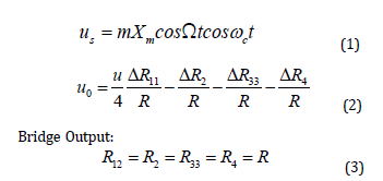
This paper aims to design a gesture recognition system based on bend sensors, which accurately identifies user gestures by capturing the bend sensor signals generated from different hand movements. The system design encompasses both hardware and software components. In terms of hardware, elements such as bend sensors, modulation and demodulation circuits, analog switch circuits, amplification circuits, filtering circuits, AD conversion circuits, and audio-visual alert circuits are designed and implemented. Signal Acquisition and Processing Circuitry is responsible for measuring, converting, and processing the bending angle signals. To convert the resistance changes of the sensor into voltage signals and improve the anti-interference capability, the flex sensor 4.5 bend sensor is chosen in this sys tem, along with a single-arm bridge circuit as the conversion circuit. To achieve sequential measurements of the five fingers for gesture recognition, an analog switch selection circuit is designed. After amplification, signal modulation, and recovery processing, the signal is ultimately converted to a digital signal using an AD conversion circuit. Additionally, the system has been programmed to accommodate a single finger as a substitute for the multiple fingers used during experimentation. The system is also equipped with an audio-visual alerting circuit, along with its driving circuit and a digital display circuit. The power supply section of the entire system is powered by a dual power supply of positive and negative 5V. Figure 1. The simulation of bend angle measurement for a single finger is depicted in Figure 2.
Based on the data presented in Figure 2, the resistance value of the flex sensor is approximately 11.5kΩ. The output signal of the sensor bridge is represented by the red line and exhibits a sinusoidal AC signal with a frequency of 500Hz and an amplitude of 0.3V. This signal is then input to the ADC, resulting in the generation of a DC signal depicted by the blue line, which is approximately 2V. Subsequently, through the conversion performed by the AD module with a reference voltage of 5V, the obtained digital output is 01101010, or 100 in decimal representation. This paper focuses on the gesture recognition of a single finger, while future work can involve programming to enable recognition of gestures from all fingers. Figure 3. According to the description in Figure 3, the system assigns numbers 1 to 5 to the five fingers, corresponding to the binary- coded octal digits D1 toD6. Gesture 1 corresponds to D2 being high, gesture 2 corresponds to both D2 and D3 being. high, and so on. However, gesture 9 has a unique characteristic that requires further subdivision of the second finger with number 2. Specifically, if all three joints are not bent, D0 is 0 and D2 is 0; if the first two finger joints are bent, D0 is 1 and D2 is 0; if all three finger joints are bent, D0 is 0 and D2 is 1. In conclusion, the system obtains the codes corresponding to the ten gestures from 1 to 10, as shown in Table 1 below.
Table 1: Gesture Codes.

Figure 1: presents the overall design of the system and the schematic diagram of the simulation circuit.

Figure 2: illustrates the simulated signals at arbitrary angles ranging from 0° to 90°.

Figure 3: depicts the process of gesture code formulation, along with illustrative diagrams of the corresponding hand gestures.

Circuit Design and Simulation
Based on the aforementioned principles and requirements analysis, this system has meticulously designed a series of circuit modules, encompassing signal acquisition, analog switches, modulation-demodulation, amplification, low-pass filtering, AD conversion, driving, and audio-visual alarm functions. The following sections will present the design schemes for each part in detail.
Signal Acquisition and Analog Switch
Figure 4: Circuit Connection of ADG407 Analog Switch Chip.

In the signal input section of this system, considering the need to simultaneously process input information from five fingers, precise control over the on-off states of signals passing through the five-channel bridge outputs is necessary. To achieve this objective, a strategy of multiplexed channel sampling can be employed, efficiently utilizing signal conditioning and the shared ADC section for effective data processing. In this system, we introduce ADG407, an 8-to-1 differential analog switch, as shown in Figure 4. The input terminals S1AS5A and S1BS5B of this switch are connected to the dual outputs of the five bridges. By utilizing this switch, we can flexibly choose one set of input signals and route them to the output terminals DA and DB. These two output terminals are connected to the input of the amplifier for amplification of the selected input signal. To effectively control the ADG407 analog switch, we connect the address lines A0 A2 and the enable pin EN to the microcontroller’s IO ports. By carefully manipulating these pins, we can flexibly control the ADG407, enabling its on- off states and link selection, thereby efficiently managing the connectivity and disconnection of input signals. Figure 4.
Modulation
To effectively process signals, this system employs amplitude modulation to convert signals into modulated ones. After modulation, the signal is amplified, filtered, and subsequently subjected to demodulation. In this system, we opt for modulation with a carrier frequency of 500Hz. To achieve modulation and demodulation, this system employs amplitude modulation and corresponding simple modulation-demodulation circuit principles.
This system utilizes a fixed resistor of 9kΩ and a sliding potentiometer ranging from 0 to 5kΩ to simulate the variation in bending degree. Figure 5.
Figure 5: Sensor Modulation and Waveform Display.

Amplification
Prior to the amplification circuit module, this system includes a modulation circuit to amplify the output signal of the modulation circuit. This modulation circuit utilizes AC electrical signals to achieve sensor modulation. In the system, the bend sensor is connected to one end of the bridge, and when the bridge becomes unbalanced, there is a voltage. difference across the bridge arms. To enhance this differential signal, the AD623AR differential amplifier was chosen. Its inverting and non-inverting inputs are connected to the two bridge arms, achieving signal amplification through differential amplification. Figure 6. Following the amplification circuit module, the signal undergoes processes such as bandpass filtering, envelope detection, and low pass filtering before AD conversion. To ensure an appropriate signal level input to the ADC, the amplification factor of the amplification circuit needs to be determined. Through simulation design, this system concludes that when the amplification factor of the amplification circuit is set to 3, the maximum output signal is around 3.8V. Meanwhile, when the resistances of the two bridge arms are equal, i.e., at the minimum signal output, it is in the order of microvolts, satisfying the conditions for AD acquisition. Thus, we confirm the amplification factor of the amplification circuit as 3 Figure 7. The amplification circuit amplifies the maximum output signal threefold, resulting in a maximum value of around 1.6V. After undergoing subsequent demodulation and filtering circuits, the DC signal size is approximately 3.8V, meeting the requirements for AD sampling values Figure 8.
Figure 6: Amplification Circuit Structure.

Figure 7: Amplification of Maximum and Minimum Output Signals.

Figure 8: Maximum Value Entering AD Sampling.

Filtering
Figure 9: Computer Aided Simulation of Bandpass Circuit.

Figure 10: Bandpass Filtering and Amplitude-Frequency Characteristics at 500 Hz.

In this system, a bandpass filter needs to be designed to effectively suppress noise interference. Through computer- aided simulation, appropriate components can be selected for subsequent production practices, providing design references. Figure 9. During the initial design phase, using a signal generator, signals of 500 Hz and 50 Hz are provided, and simulated curves in the frequency domain and time domain are obtained using a Bode analyzer and an oscilloscope. Figure 10. At a frequency of 500 Hz, within the passband, the amplitude is 5.874 dB, meeting the target of doubling the amplification within the passband, in accordance with system requirements. Figure 11. At a frequency of 50 Hz, the stopband is reached, with an amplitude of -49.857 dB, resulting in an output signal less than one three-hundredth of the original signal, effectively filtering out noise such as power frequency interference Figure 12. During the overall circuit integration, this bandpass filter achieves the desired function of doubling the amplification within the passband.
Figure 11: Bandpass Filtering and Amplitude-Frequency Char acteristics at 50 Hz.

Figure 12: Bandpass Filtering Circuit Effect during Integration Testing.

Demodulation Circuit
Figure 13: Rectification Circuit Waveform Display.

a. Full-Wave Precision Rectification Circuit: This system employs a full-wave precision rectification circuit to ensure the complete positive inversion of analog voltage signals caused by changes in
b. Low-Pass Filtering Circuit: To enhance the first-order filtering effect of the original demodulation circuit and reduce the sharpness of the demodulated output signal, this system employs a second-order voltage-controlled low-pass filtering circuit to replace the capacitor in the feedback channel of the original demodulation circuit Figure 14. From the amplitude-frequency characteristics curve, it can be observed that a gain amplification of 2 within the passband and an expected 3 dB attenuation at the cutoff frequency of 10 Hz can be achieved Figure 15 During the overall circuit integration, this low-pass filter assists the envelope precision rectification circuit in achieving signal demodulation (indicated by the red line in Figure 15.
Figure 14: Computer-Aided Simulation of Low-Pass Circuit and its Amplitude-Frequency Characteristics.

Figure 15: Effect of Bandpass Filtering Circuit during Integration Testing.

AD Conversion
To realize a gesture-based intelligent recognition system using bend sensors, it is necessary to convert the bridge’s output signal into an analog voltage signal. For this purpose, an interface circuit, such as an A/D converter or D/A converter, needs to be added to convert the analog signal into a digital signal for subsequent display and storage processing. This system chooses the 8-bit ADC converter ADC0809 chip. Taking the A/D conversion circuit (ADC) as an example to build the analog-to-digital conversion circuit, the ADC can convert the input analog signal into an 8-bit digital signal output Figure 16. When the resistance is adjusted to 80% of the original resistance value, we can observe the digital signal indicators. X3, X6, and X8 are lit, indicating that the voltage value has been converted to the digital value 00100101. When the resistance is adjusted to 100% of the original resistance value, we can observe that the digital signal indicators X1, X3, X7, and X8 are lit, indicating that the voltage value has been converted to the digital value 10100011. By using the binary number obtained from the AD conversion as the segment code for the digital display, we can show the specific gesture value on the digital display, achieving a visual representation of gesture recognition.
Driving and Audio-Visual Alarm
The driving and audio-visual alarm circuit are used to implement sound and light display and alarm functions controlled by the microcontroller. This includes LED circuits and buzzer circuits, along with their corresponding driving circuits. To meet the requirement of a load current less than 500mA, this system uses a transistor power switch driving circuit. In this driving circuit, the 2N 3904 transistor is chosen as the switching element. The 2N 3904 is a commonly used small- signal NPN-type transistor, with a collector current of up to 200mA and a gain range of 100 to 300. This choice ensures the reliability and performance of the driving circuit. Figure 17. When the microcontroller’s IO port outputs a high level (V EE is high, i.e., logic level is 1), the LED will light up, and the buzzer will emit a beep. However, through measurement, it was found that the buzzer and LED currents are 31mA and 11mA, respectively, with a slight discrepancy from theoretical calculations. When the microcontroller’s IO port outputs a low level (V EE is low, i.e., logic level is 0), the LED will turn off, and the buzzer will not beep. In this case, a clamping diode D1 is connected in parallel to address the issue of reverse voltage caused by the buzzer acting as an inductive component. This design takes into account the circuit’s stability and the requirement to protect the buzzer component. trical bridge bending angle
Figure 16: AD Conversion Simulation at 80% and 100% of Original Resistance.

Figure 17: Single-Microcontroller IO Output High and Low Levels.

Experimental Results and Analysis
The experimental setup of the gesture intelligent recognition system under study in this paper is constructed based on a breadboard. The primary tasks include programming and debugging of analog switch circuits, which constitute the foundation of the system. The system design encompasses key components such as modulation-demodulation circuits, ampli fication circuits, analog switch circuits, band-pass filtering AD conversion, and audio-visual alarm circuits. During the practical construction and debugging process, a sequential integration is followed, involving the sensor modulation interface circuit, amplification circuit, analog switch circuit, band-pass filtering circuit, demodulation circuit, AD conversion circuit, and audio-visual alarm drive circuit. In order to showcase the experimental results, an oscilloscope and a microcontroller are employed. In the experiment, oscilloscope and microcontroller are utilized to present experimental outcomes.
Modulation and Demodulation Circuit
In the demodulation circuit, the system designed in this study employs a sensor bridge modulation method. The specific procedure involves introducing a 500Hz high-frequency signal at the ends of the bridge, with the other two ends serving as feedback signals. The bridge comprises four arms, wherein one arm is connected to a bending sensor, another arm is linked to a resistor with a resistance similar to that of the sensor, and the remaining two arms are connected to resistors of identical values. During the experiment, it was observed that due to multiple deformations of the bending sensor, its inherent resistance in the un-bent state cannot be perfectly matched, leading to a weak output from the bridge in the un-bent condition. After amplification, the output of the bending sensor is depicted in Figure 18. As the bending angle increases and the resistance of the sensor rises, the feedback signal is amplified by the differential amplifier, causing the voltage to gradually rise, as illustrated in (Figures 18 & 19).
Figure 18: The amplified output trical bridg.

Figure 19: Increase in volt- of the unbent state of the elecage variation with increasing bending angle.

In the modulation circuit, the system designed in this study has adopted the envelope detection method. As per the design simulation, as shown in Figure 20, and successfully realized in physical construction. During the experiment, a 20Hz sine wave with a maximum peak level of 3V and a minimum trough level of -3V was fed into the detection circuit. The observed results indicated a fully upturned waveform, successfully achieving the detection function, as depicted in Figure 21 Utilizing a single-bridge bridge circuit design, when the sensor is in an un-bent state, the output voltage amplitude of the bridge arms is small, resulting in a weak signal after amplification. However, bending the sensor leads to an imbalance in the bridge arms, increasing the output signal amplitude, with a more pronounced variation after passing through the amplification circuit. Observing the demodulated output on the oscilloscope and the lowpass filtered output on the oscilloscope, the blue signal represents the waveform after demodulation. This demodulation method causes the sinusoidal signal to fold, resulting in exclusively positive half-wave signals. After filtering the demodulated signal, the experimental results yield its average value signal, i.e., the direct current (DC) signal, as depicted in Figure 22.
Figure 20: Envelope detection circuit design schematic.

Figure 21: Envelope detection output signal waveformCH12.00V 100Hz.

Figure 22: Detection and low pass filtering results.CH1 500mV CH2 500mV 1,00ms.

Amplification Circuit
Figure 23: Operational amplifier (op-amp) configuration simula tion schematic.

Figure 24: Amplifier circuit schematic diagram.

Figure 25: Input signal before amplification.

Figure 26: Amplified signal CH2200mV 25ms.

Figure 27: Intermodulation amplified signal CH2 500mV 1.00ms.

To conduct the amplification circuit experiment, a three-op- amp circuit was employed and simulated using Multisim. For amplification 200mV25ms simulation purposes, the TL084 integrated circuit was used as the operational amplifier, with amplification factors of 3 (first stage) and 1 (second stage), resulting in a total gain of 3. In accordance with the project requirements, corresponding structural simulation diagrams and amplification circuit schematics were drawn, as illustrated in (Figures 23 & 24) Based on the schematic diagram, the circuit was constructed using a breadboard, and connections were made to the Mul- tisim simulated circuit for debugging. After debugging and observation, the amplification circuit achieved a threefold amplification with minimal error and interference. A signal generator was used to input a 10Hz frequency signal with an amplitude of 250 millivolts, and the output waveform of the amplification circuit was observed on an oscilloscope, as shown in Figure 25. The amplification circuit successfully achieved the intended effect, generating a sinusoidal amplified signal with an approximate amplitude of 750 millivolts, as demonstrated in Figure 26. Considering that the signal source of the amplification circuit originates from the modulation signal of the sensor bridge, it was initially calibrated with the output signal of the bridge. After successfully adjusting the corresponding connections, it was then connected to the second-stage band- pass filter, with the calibration results depicted in Figure 27
Bandpass Filter
Figure 28: Cascade of low-order bandpass filter circuit.

Figure 29: Input and output of cascade of low-order bandpass filters 5V pp1V 500μsIm = 3.04V.

Figure 30: Prototyping a low-pass circuit on a breadboard.

Figure 31: Output at the cutoff frequency of the low-pass circuit Im = 5.24f = 6.33Hz.

Figure 32: Output of detection and low pass filtering CH1 500mV CH2 500mV M1ms.

Figure 33: Output after intermodulation bandpass filtering CH1 500mV.

Figure 34: Output after intermodulation low pass filtering Im=140mV.

In the band-pass filtering section, a first-order high-pass and a first-order low-pass cascaded band-pass filter circuit were employed in this study, as depicted in Figure 28. Despite its moderate performance with an attenuation of approximately one magnitude within the passband, it still fulfills the basic band-pass functionality, as demonstrated in Figure 29. Within the passband, an approximate one-magnitude attenuation is observed, effectively filtering out other interferences within the stopband. To enhance demodulation efficiency, an independent second-order voltage-controlled voltage source low-pass filter was employed after demodulation to eliminate the carrier signal. Utilizing the available laboratory components, the circuit was constructed as shown in Figure 30. This filter possesses. a cutoff frequency of 5Hz and a passband gain of k=2. The gain at the carrier frequency of 500Hz is approximately. -70dB, thereby satisfying the carrier removal design require ment. Experimental results are detailed in Figure 31requirementompletion and testing of each individual circuit section, an overall circuit integration and calibration were conducted. The output results of the demodulation and low- pass filtering is presented in Figure 32. As the bending sensor undergoes a certain degree of bending, the output voltage undergoes variation, triggering the alarm of a buzzer. The outcomes of the integration and calibration are elaborated in Figure 33 and Figure 34, confirming the proper functionality of the modulation circuit designed in this study.
AD Conversion
The AD conversion section of this circuit employs the ADC0809 chip as the analog-to-digital converter, as shown in Figure 35. Within the ADC0809 module, the jumper values at J3, J4, and J5 can be manually set to activate the corresponding input channels. Furthermore, potentiometer R1 is introduced to adjust the voltage value of input channel 3, as illustrated in PCB diagram 36. During the individual debugging of the ADC0809, by adjusting the potentiometer, it was observed that the value on the digital display changes linearly and maintains a well- corresponding relationship with the input voltage value.
Figure 35: Analog-to-digital schematic.

Figure 36: Analog-to-digital con- conversion module design version module PCB layout diagram.

Drive And Audio-Visual Alarm
Based on the design schematic, the schematic diagrams for driving and audio-visual alarm circuits were drawn using Altium Designer, with the drawing results shown in Figure 37. This schematic diagram is fundamentally consistent with the designed circuit diagram. Additionally, for convenient interfacing with the preceding circuits, an extra four-pin header was added to lead out the control terminals of the two driving circuits, as well as the power supply V CC and GND. During the PCB design phase, both the bottom and top layers were drawn. Initially, the components in the schematic were encapsulated and logically placed within the overall layout. Subsequently, wiring operations were conducted, with vertical lines arranged on the top layer and horizontal lines on the bottom layer. Finally, copper traces were laid out to form the final board, as depicted in Figure 38. The actual working diagram is presented in Figure 39 the left side shows the state when the microcontroller-controlled IO outputs a low level, with the buzzer and LED in a non- operational state; the right side demonstrates the state when the microcontroller-controlled IO outputs a high level, with the LED and buzzer functioning normally. The observed effect is satisfactory and aligns with the anticipated design requirements. Finally, the AD conversion and audio-visual drive stages were executed. When the sensor is bent, the output DC signal increases to over 2 volts. At this point, under the control of the microcontroller, the system designed in this study successfully accomplishes functions such as buzzer alarms and LED illumination. Simultaneously, the corresponding output voltage value is displayed on the digital display, as illustrated in Figure 40.
Figure 37: Driver circuit schematic diagram.

Figure 38: Final product diagram.

Figure 39: Output of detection and low pass filtering CH1 500mV CH2 500mV M1ms.

Figure 40: Corresponding gesture voltage value display effect.

Conclusion
The article presents a gesture intelligent recognition system based on bend sensing technology. This system successfully tackles the challenge of balancing cost and accuracy, achieving gesture recognition with both low cost and high precision. This innovation has significant implications in areas such as human-computer interaction and healthcare. Future research will focus on overcoming the limitations of gesture recognition technology in practical application scenarios and alleviating the inconvenience of wearable devices. Additionally, efforts will be made to improve recognition precision and intelligence, reduce device costs, and promote the widespread adoption of intelligent gesture recognition technology.
References
- Yuting Liu, Du Jiang, Haojie Duan, Ying Sun, Gongfa Li, et al. (2021) “Dynamic Gesture Recognition Algorithm Based on 3D Convolutional Neural Network”. Computational Intelligence and Neuroscience pp. 12.
- Gao P (2022) Key technologies of human-computer interaction for immersive somatosensory interactive games using VR technology. Soft Comput 26: 10947-10956.
- Asadzadeh P, Kulik L, Tanin E (2012) Gesture recognition using RFID technology. Pers Ubiquit Comput 16: 225-234.
- Mitra S, Acharya T (2007) Gesture recognition: a survey. IEEE Transactions on Systems, Man, and Cybernetics-Part C: Applications and Review 37(3): 2127-2130.
- Chaudhary A, Raheja JL, Das K, Raheja S (2011) A Survey on Hand Gesture Recognition in Context of Soft Computing. Advanced Computing pp. 46-55.
- Xie X, Zhang S, Wu J, Xu X, Shi G, et al. (2019) A Real- Time Rock-Paper-Scissor Hand Gesture Recognition System Based on FlowNet and Event Camera. Pattern Recognition and Computer Vision pp. 98-109.
- Chu X, Liu J, Shimamoto S (2021) A Sensor-Based Hand Gesture Recognition System for Japanese Sign Language. 2021 IEEE 3rd Global Conference on Life Sciences and Technologies (LifeTech) pp. 311-312.
- Liang X, Heidari H, Dahiya R (2017) Wearable Capacitive-based Wrist-worn Gesture Sensing System. In New Generation of Circuits and Systems Conference (NGCAS 2017) pp. 181-184.
- Zhang W, Zhang J (2022) EMG Gesture Recognition Algorithm Based on Parallel Multi-scale CNN. 2022 2nd International Conference on Frontiers of Electronics, Information and Computation Technologies (ICFEICT) pp. 562-568.
- Xu Zhang, Xiang Chen, Zhang-yan Zhao, You-qiang Tu, Ji-hai Yang, et al. (2007) Research on Gesture Definition and Electrode Placement in Pattern Recognition of Hand Gesture Action SEMG. Medical Biometrics pp. 33-40.
- Taiqian Wang, Yande Li, Junfeng Hu, Aamir Khan, Li Liu, et al. (2018) A Survey on Vision-Based Hand Gesture Recognition. Smart Multimedia pp. 219-231.
- Fang W, Ding Y, Zhang F, Sheng J (2019) Gesture Recognition Based on CNN and DCGAN for Calculation and Text Output. IEEE Access (7): 28230-28237.
- Geer D (2004) Will gesture recognition technology point the way?. in Computer 37(10): 20-23.
- Yun L, Peng Z (2009) An automatic hand gesture recognition system based on Viola-Jones method and SVMs. IEEE.
- Kakumanu P, Makrogiannis S, Bourbakis N (2007) A survey of skin-color modeling and detection methods. Pattern Recognition 40(3): 1106-1122.
- Josue´ Espejel Cabrera, Jair Cervantes, Farid Garcıa Lamont, Jose´ Sergio Ruiz Castilla, Laura D Jalili (2021) Mexican sign language segmentation using color based neuronal networks to detect the individual skin color. Expert Systems with Applications 183: 115295.
- Andersen MR, Jensen T, Lisouski P, Mortensen AK, Hansen MK, et al. (2012) Kinect Depth Sensor Evaluation for Computer Vision Applications. Pp. 37.
- Rodrigo Iban ez, lvaro Soria A´, Alfredo Teyseyre, Marcelo Campo (2014) Easy gesture recognition for Kinect. Advances in Engineering Software 76: 171-180.
- Danilo Avola, Luigi Cinque, Alessio Fagioli, Gian Luca Foresti, Adriano Fragomeni, et al. (2022) 3D hand pose and shape estimation from RGB images for key point-based hand gesture recognition. Pattern Recognition 129: 108762.
- Hermann Baumgart, Daniel Sauter, Christian Schenk, Cem Atik, Ricardo Buettner, et al. (2021) Vision-based hand gesture recognition for human- computer interaction using MobileNetV2. IEEE.
- Thippa Reddy Gadekallu, Gautam Srivastava, Madhusanka Liyanage, Iyapparaja M, Chiranji Lal Chowdhary, et al. (2022) hand gesture recognition based on a Harris Hawks optimized Convolution Neural Computers and Electrical Engineering 100: 107836.
- Yong Soon Tan, Kian Ming Lim, Chin Poo Lee (2021) Hand gesture recognition via enhanced densely connected convolutional neural network,Expert Systems with Applications,Volume 175: 114797.
- Gong Li, Dongxu Bai, Guozhang Jiang, Du Jiang, Juntong Yun, et al. (2023) Continuous dynamic gesture recognition using surface EMG signals based on blockchain-enabled internet of medical things. Information Sciences 646: 119409.
- Byun SW, Lee SP (2019) Implementation of hand gesture recognition device applicable to smart watch based on flexible epidermal tactile sensor array [J]. Micromachines 10(10): 692.
- Barbhuiya AA, Karsh RK, Jain R (2021) CNN based feature extraction and classification for sign language. Multimed Tools Appl 80(2): 1-19.
- Wei Gu, Shengchang Yan, Jian Xiong, Yaogang Li, Qinghong Zhang, et al. (2023) Wireless smart gloves with ultra-stable and all-recyclable liquid metal- based sensing fibers for hand gesture recognition. Chemical Engineering Journal 460: 141777.


-

Mark E Smith
Bio chemistry
University of Texas Medical Branch, USA -

Lawrence A Presley
Department of Criminal Justice
Liberty University, USA -

Thomas W Miller
Department of Psychiatry
University of Kentucky, USA -

Gjumrakch Aliev
Department of Medicine
Gally International Biomedical Research & Consulting LLC, USA -

Christopher Bryant
Department of Urbanisation and Agricultural
Montreal university, USA -

Robert William Frare
Oral & Maxillofacial Pathology
New York University, USA -

Rudolph Modesto Navari
Gastroenterology and Hepatology
University of Alabama, UK -

Andrew Hague
Department of Medicine
Universities of Bradford, UK -

George Gregory Buttigieg
Maltese College of Obstetrics and Gynaecology, Europe -

Chen-Hsiung Yeh
Oncology
Circulogene Theranostics, England -
.png)
Emilio Bucio-Carrillo
Radiation Chemistry
National University of Mexico, USA -
.jpg)
Casey J Grenier
Analytical Chemistry
Wentworth Institute of Technology, USA -

Hany Atalah
Minimally Invasive Surgery
Mercer University school of Medicine, USA -

Abu-Hussein Muhamad
Pediatric Dentistry
University of Athens , Greece