


Lupine Publishers Group
Lupine Publishers
ISSN: 2641-6921
Research Article(ISSN: 2641-6921) 
Elastic Wave Propagation Research on Two-Dimensional Photonic Crystal Structures of W-Silicone Rubber Volume 2 - Issue 5
Received: March 05, 2020; Published: March 16, 2020
*Corresponding author: Dongxing Cao, College of Mechanical Engineering, Beijing University of Technology, Beijing, China
DOI: 10.32474/MAMS.2020.02.000147
Abstract
The two-dimensional phononic crystal structures of W-silicone rubber are designed here for the low-frequency vibration absorption by applying both the plane wave expansion method and finite element method. The band structures of phononic crystal are calculated and some special phenomena in the band structures are discussed, such as the Dirac point and the degenerate state near the Dirac point and so on. Moreover, the main deformations of different modes for the structure are given, which indicated that the stress concentration is easy to occur in joint parts of the matrix and scatter. Furthermore, the influence of different parameters on the band gaps of the phononic crystal is discussed by finite element method, including the density ratio and the Young’s modulus ratio. At last, the defect state of two-dimensional phononic crystal is visualized which verifies that acoustic wave can propagate along point defect or line defect of the system. The results will provide certain theoretical guidance for engineering application.
Keywords:W-silicone rubber Phononic crystal; Plane wave expansion method; Degenerate states; Defect state
Introduction
Phononic crystal are periodic function materials composed of two or more than two different mechanical properties materials. The most important characteristic of these structures is the existence of phononic band gaps [1-3], which mean some specific frequency ranges of elastic wave propagation can’t pass through the structures. Therefore, the phononic crystal structures have a broad application prospect, for example, vibration isolation, vibration acoustic, noise reduction, isolator waveguide filter device and so on [4-9]. Researches on phononic crystal structures are mainly concentrated on the propagation performance of elastic wave in different phononic crystal structures. For example, Sorokin et al. [10] considered these phenomena in periodic plates and cylindrical shells with and without heavy fluid loading. Romeo et al. [11,12] present general three-coupled phononic crystal structures through the transfer matrix method. Li et al. [13] introduced a microscale cavity for the two-dimensional phononic crystal. Shan et al. [14] analyzed the propagation of elastic waves in porous phononic crystal structures. Baravelli et al [15] designed a beamlike assembly with a stiff external frame and an internal resonating lattice, which was characterized by high frequency band gaps and tuned vibration attenuation at low frequencies. Zhang et al. [16] discussed the band gaps and damping characteristics of thin plate phononic crystals. The application of complex phononic crystal structures are also reported in some fields, for example, Huang et al. [17] showed its application in semi-active control and health monitoring of intelligent structures. Huang et al. [18] analyzed the electromagnetic wave absorption characteristics of aluminum gradient phononic crystal structures. Li et al. [19] researched the low frequency vibration isolation characteristics of local resonant phononic crystal plates. Wan et al. [20] proposed a low frequency noise attenuation system based on phononic crystal structures and discussed the effects of structure parameters on the band gaps. Zou et al. [21] showed the decoupling of two coupled phononic crystal waveguides M. Zubtsov et al. [22] designed a normal incidence phononic crystal sensor and analyzed its characteristics. Another important researches for phononic crystal structures are the analyzed methods to calculate the band structures. Some calculation methods have been developed, such as transfer matrix method, plane wave expansion method, time-domain finite difference method, multiple scattering method and finite element method, etc. [23-26].
Mention to the different characters of these methods, the transfer matrix method is more suitable to calculate the band structures of one-dimensional phononic crystals [27]. The planewave expansion method has a clear physical concept and high computational efficiency, which are widely applied to obtain the band structures of two-dimensional phononic crystals [28]. Finitedifference time-domain method can be used to more complex models [29] but requires a lot of computation. The theoretical derivation of multiple scattering method is relatively complicated and only used for phononic crystals with simple cylindrical and spherical scattering element structures [30]. The finite element method can not only calculate the band structures, but also quickly obtain the transmission loss of the phononic crystals [31]. In this paper, both plane wave expansion method and finite element method are applied to obtain the low frequency band structures and transmission loss of two-dimensional square lattice solid/ solid phononic crystals. Meanwhile, the special phenomena in such band structures are analyzed. The effectiveness of low frequency vibration isolation of this structure is proved theoretically, which provides some guidance for the engineering application.
Model Introduction
Since the phononic crystals have characteristics of periodicity, one-unit cell can represent the entire structure to be analyzed for ideal phononic crystals [32]. As shown in Figure 1(a), this two-dimensional square lattice unit cell is composed osf circular scatters and square matrix, and the material of scatters and the matrix are made of tungsten and silicone rubber, respectively. The parameters are including lattice constant a and scattered radius r, and scattered fill rate is f =π r2 / a2 . Then according to Bloch’s theorem, the periodic boundary conditions are applied to the all boundaries of the unit cell, as shown in Figure 1(b), which are satisfied the boundary displacement ui( x+ a, y +a ) = ui(x, y)e-i(kx)a ky)a (i= x, y ) (u is the displacement and k is the wave vector). When the wave vector is taken along the boundary of the first Brillouin zone, which means it is scanned along the direction Γ − X −M − Γ as shown in Figure 1(c). The characteristic frequencies of the structure are obtained by solving the eigenvalue problem to analyze the band structures of the phononic crystal structures (Figure 1). Then, the numerical simulation model is applied to calculate the transmission loss of the structure, as shown in (Figure 2).
Figure 1: (a) A cell diagram (b) a boundary condition relationship (c) the first Brillouin region.

Figure 2: A finite structure containing 10-line elements for calculating transmission losses.

Taking the ΓΧ direction as an example, the phononic crystal contains 10unit cells in the x direction and has an infinite periodic structure in the y direction, where the Bloch periodic boundary condition is supposed to be in the upper and lower sides of the y direction. An absorptive boundary condition for the perfectly matched layer is constructed at both ends of the x direction. To calculate of the transmission spectrum, a background sound pressure is exerted at the incident section first, whose unit pressure is 1Pa. The incident wave would propagate through 10 rows of cells in the x direction. Then receivers for measuring the sound pressure are put at the incident section and exit section, respectively. Moreover, the transmission loss is defined as the logarithmic ratio of the squared value of the transmitted sound pressure through the 10-layers finite system to the square of the incident sound pressure, written as TL =10log10( p2in/ p2out) where pin is the incident sound pressure and pout is the transmitted sound pressure.
Introduction of the Plane Wave Expansion Method
The plane wave expansion method is one of the most commonly methods for calculating the elastic wave band gaps of phononic crystals with different dimensions. Its basic idea is to expand the material and structural parameters of the phononic crystals to the Fourier series, and then superimpose the plane waves in the reciprocal vector. The band structures are obtained by the approximate solution of the space. Due to the periodicity of the phononic crystals, the Lame constants (λ andμ )and the density ρ are periodic functions of the space r = (x, y) , and each parameter can be expanded according to the Fourier series. For the convenience of description, these three parameters are uniformly expressed as follows
 (1)
(1)
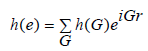
where h(G) is the parameter of Fourier series, G is reciprocal vector and can be defined as follows for the two-dimension crystal lattices
G= n1b1 + n1b1 (2)
Here, n1 and n2 are integers, b1 and b2 means the basic vectors for G.
The parameters for the h(G) in Eq (1) are calculated by
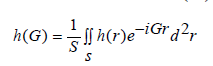 (3)
(3)
Here, S means the area of the unit cell. When G = 0 , Eq. (3) satisfied the following equation,
h(G) = hAf + hB(1− f) (4)
where f is the filling ratio of the scatter in the unit cell, hA and
hB are the corresponding parameters for the scatter and matrix,
respectively.
IfG ≠ 0 , then
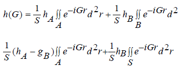 (5)
(5)
Based on the boundary condition of the periodicity, the integral of the second term for Eq.5 becomes zero, that is
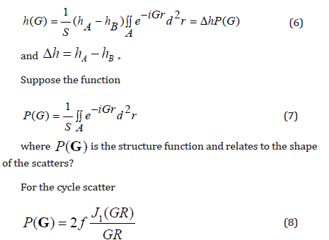
where J1 is the first order and type of Bessel function, andG is
the model of the reciprocal vector.
Then, based on Eqs. (4) and (6), the parameter h(G) is
rewritten as follows
 (9)
(9)
The displacements are expressed in the following form by the Bloch theorem
u(r, t)= ei(kr-ωt)uk(r) (10)
where k is the Bloch wave vector, confined within the first Brillouin zone (see Figure 1(b)). uk(r) are the functions with same periods of each material parameter and can be expanded into a Fourier series, that is,
 (11)
(11)
Substitute Eq. (11) into Eq. (10), then
u(r, t)= ei(G+k)r uk (G ') (12)
Finally, the eigenvalue equation can be obtained by further calculation
 /p>
/p>
Then, the band structures of W-silicone rubber phononic crystal structures are obtained by MATLAB based on the obtained eigenvalue equation (13). In this paper, 961 plane wave numbers are selected.
The Results and Discussion
The Band Structure of a Unit Cell
Choose the scattered radius of the single cell structure as 4mm and the lattice constant as 10mm, and material parameters are shown in Table 1. The band structure of unit cell for the twodimensional W-silicone rubber phononic crystal is obtained with two different methods, which shown in Figure 3. The pink curve is the result simulated by finite element method (FEM), while the blue one is the calculation by the plane wave expansion method (PWE). It is easy to find that the range of the first complete band gap calculated by PWE is 382Hz-997Hz, the bandwidth is 615Hz and its center frequency is 689.5Hz. Meanwhile, the range of the same gap by the FEM is from 396.9Hz to 1009.4Hz, the bandwidth is 639.5Hz and its center frequency is 703.15Hz. Therefore, the results of these two methods basically agree with each other, which verify the correctness of the calculation by PWE. Figure 3 also presents that there are multiple incomplete band gaps in the first Brillouin region of the phononic crystals composed of W-silicone rubber. The band gaps appear in the range of middle and low frequencies, such as the first complete band gap. The existence of such gaps has a certain guiding effect on the isolator design of mid- and low-frequency vibrations in engineering. Moreover, the sixth and seventh energy bands intersect and form a double degenerate Dirac point in the Brillouin zone boundary of the XM direction.
Table 1: Material parameters.

Figure 3: Two-dimensional band structure of periodic structure of w-silicone rubber.

To present the existence of Dirac points clearly, enlarge the shadows locally of (Figure 3), it is found that Dirac points exist in the system by both the PWE and FEM, but the positions are slightly different. Meanwhile, all directions except the XM direction occur in forbidden band. In order to analyze the cause of the Dirac point in the band structure further, the eigen field diagram of the double degenerate state of the two-dimensional phonon crystal at the Dirac point frequency is calculated, and results are shown in (Figure 4). Pictures 4(a) and 4 (b) are the dipole state and the quadrupole state, respectively, both of which are belong to the double degenerate states. Since the eigen field diagram are consistent with the band structure, this double degeneracy leads to the appearance of Dirac points. Based on the band structure of unit cell for the two-dimensional W-silicone rubber phonon crystal, the ten cells of W-silicone rubber phononic crystal models are designed to verify if the same phononic band gaps exist in the super cell structure of a finite unit cell combination. The transmission loss of the structure is shown in (Figure 5). The cyan range is the forbidden band, which is from 475Hz to 1000Hz. The bandwidth is 525Hz and the center frequency is 737.5Hz. The results are basically consistent with the obtained calculation of the single-cell energy band of the two-dimensional W-silicone rubber phononic crystal. It is proved that the above phononic crystal has the same range of the band gaps between the unit cell and the super cell. The research on the unit cell can be extended to the super cell structure, which is extremely beneficial for simplifying the calculation process. To analyze the relationship between frequency and wave vector more intuitively, (Figure 6) gives the three-dimensional map of the first energy band of the phononic crystal and its two-dimensional cloud image. Moreover, the frequency of wave vector is 0 at the position of the higher symmetric point τ, and has a larger frequency rang in the XM direction. The deformation trend of the W-silicone rubber phononic crystal is analyzed in different modes to guide the engineering practice.
Figure 4: Eigenstate pressure field of structure (a)quadrupole states (b) dipole state.

Figure 5: Transmission loss of super cellular structure.

Figure 6: Three-dimensional map of the first energy band and its two-dimensional cloud map.

Figures 7a & 7b show the change trend of total displacements of modes A and B (corresponding to mode A and mode B in Figure 3), respectively. It is found that mode A mainly undergoes torsional deformation and mode B is shear deformation. Moreover, the deformation in the center and four corner positions of the unit cell is small for the mode A, however, the one at the junction of the scattered and the matrix is large. For mode B, the deformation of the four corner positions is large and that of the scattered is relatively uniform. Therefore, the connection between the scattered and the matrix is a stress concentration area for torsional deformation, and the effect of shear deformation on the scattered is not obvious. The connection part of the scattered and the matrix needs to be reinforced in engineering applications (Figure7).
Figure 7: Change of total displacement nephogram (a) mode A (b) mode B.

Effects of Material Parameters on Bandgap
Another effect factor for the two-dimensional phonon band gaps is material parameters, here, 10 different scatter materials are selected in Table 2 (parameters of various materials are given). The influence of different material parameters in the phononic crystal structures on the band gaps are analyzed, includes the density ratio of the scattered to the matrix and the Young’s modulus ratio. (Figure 8) presents the effect of different density ratios on the first complete band gap of the two-dimensional solid/solid phononic crystal. When the density ratio (the ratio of the density of the scatter to the matrix) increases, the starting frequency of the first complete band gap gradually increases and the cut-off frequency changes little. Then, the bandwidth gradually decreases. Therefore, through selecting the appropriate density ratio of scatter and matrix, a lower vibration isolation frequency and a larger vibration isolation bandwidth can be obtained for the low-frequency vibration isolation design. (Figure 9) show that there is no clear relationship between the first complete band gap of the two-dimensional solid/solid phononic crystal and the Young’s modulus ratio of the scatter to the matrix. As the Young’s modulus ratio increases, the first complete band gap varies without a common rule. Therefore, density is one of the decisive factors affecting the band gap characteristics of the two-dimensional solid/solid phononic crystal.
Figure 8: The relation between the first complete band gap and density ratio.

Figure 9: The relationship between the first complete bandgap and Young’s modulus ratio.

Table 2: Various parameters of different scatterer materials.

Visualization of Defect State Phenomena
Figure 10: A cross-sectional view of the supercell structure.

The defect state of phononic crystals have important
application in the design of acoustic devices. When a defect exists
in a periodic structure, an elastic wave of a specific frequency will
be localized within the defect or propagate along the defect to form
an acoustic waveguide. Phononic crystal defect characteristics
have the advantages of high transmission rate, low loss, and good
stability and so on, which could meet the requirements of various
acoustic frequency selection, filtering, and waveguide devices for
transmission performance. Therefore, the defect state phenomenon
of the two-dimensional phononic crystal is investigated and
visualized here, showing its intuitive image. (Figure 10) is a crosssectional
view of the supercell structure of the two-dimensional
W-silicone rubber phononic crystal, which all contains 5*10
primitive cells. Figure 10(a) is a complete structure without defects.
Figure 10(b) is a point defect structure, where 4 defect scatterers
are distributed in the third row.
Figure 9c shows a line defect structure and the third line is a
line defect scatterer. The acoustic transmission characteristics
of these three supercell structures are calculated below. (Figure
11) shows the sound field distribution of these three supercell
phononic crystal structures at frequency f=700Hz (forbidden band
range) and (Figure 12) is a three-dimensional mode diagram.
From Figures 11a & 12a, it is present that the acoustic waves of
this frequency are mainly concentrated in the first two columns
of scatters in the defect-free phononic crystal, and the rest are
reflected to the incident section and cannot continue to propagate
forward. Moreover, acoustic waves can continue to propagate
forward through point defect phononic crystal as shown in Figures
11b & 12b. The acoustic waves also propagate forward through
the line defect in Figures 11c & 12c and finally pass through the
entire phononic crystal structure. These results indicate that
acoustic waves are transmitted along point defects or line defects
in phononic crystals to achieve frequency selection.
Figure 11: A cross-sectional view of the supercell structure.

Figure 12: Three-dimensional mode diagram of supercell phononic crystal structures.

Conclusion
This paper calculates the band structure of two-dimensional
W-silicone rubber phononic crystals and analyzes the special
phenomena appearing in the structure. The influence of material
parameters on the band structure are discussed and the defect state
phenomenon of the phononic crystal structure are analyzed. The
following conclusions are obtained for two-dimensional W-silicone
rubber periodic structural composites:
a. The phonon crystal structure composed of W-silicone
rubber has band gaps in the mid-low frequency ranges. The
stress concentration is easily occurred at the junction of the
scatter and the matrix.
b. As the density ratio increases, the starting frequency of
the first complete band gap gradually increases in the twodimensional
W-silicone rubber phononic crystal, but the
cut-off frequency changes little and the bandwidth gradually
decreases. By adjusting the density of the material, the band
gap characteristics of the phononic crystal structure will be
applied in the low frequency vibration absorber. Moreover,
there is no clear relationship between the first complete band
gap and the Young’s modulus ratio.
c. Acoustic waves can propagate forward along point or line
defects.
Acknowledgement
The authors gratefully acknowledge the support of the National Natural Science Foundation of China (NNSFC) through grant Nos.11772010 and 11832002, the Funding Project for High level teachers’ team construction in Beijing municipal colleges and Universities.
Conflict of Interest
The authors declare that they have no conflict of interest with respect to the research, authorship, and/or publication of this article.
References
- KushwahaMS, Halevi P,Dobrzynski L, DjafariRouhani (1993) Acoustic Band Structure of Periodic Elastic Composites. Physical Review Letters 71(13): 2022-2025.
- Aly AH, Nagaty A, Khalifa Z (2018) Study on the Piezoelectric Material and One-Dimensional Phononic Crystal.Surface Review and Letters 26: 2.
- Kriegel I, Scotognella F, Manna L (2017) Plasmonic Doped Semiconductor Nanocrystals: Properties, Fabrication, Applications and Perspectives . Physics Reports 674:1-52.
- Wang XP, Jiang P, Chen TN, Zhu J (2015) Tuning Characteristic of Band Gap and Wave Guide in a Multi-Stub Locally Resonant Phononic Crystal Plate . AIP Advances 5(10):107-141.
- Xu K, Li Z, Zhang YL (2015) An Indirect Approach Based on Clausius–Clapeyron Equation to Determine Entropy Change for the First Order Magnetocaloric Materials . Physics Letters A 379(47-48): 3149-3154.
- Zhang G, Zhao L, Jiang Z (2011) Surface Stress-Induced Deflection of a Microcantilever with Various Widths and Overall Microcantilever Sensitivity Enhancement via Geometry Modification . Journal of Physics D: Applied Physics 44: 42.
- Wang YF, Wang YS (2013) Complete Band Gaps in Two-Dimensional Phononic Crystal Slabs with Resonators . Journal of Applied Physics 114: 4.
- JinY, Torrent D, Pennec Y, Pan Y (2015) Simultaneous Control of the S0 and A0 Lamb Modes by Graded Phononic Crystal Plates . Journal of Applied Physics 117: 24.
- Benchbane S, Gaiffe O, Salut R (2015) Guidance of Surface Waves in a Micron-Scale Phononic Crystal Line-Defect Wave Guide . Applied Physics Letters 106: 8.
- Sorokin S V, Ershova OA (2004) Plane Wave Propagation and Frequency Band Gaps in Periodic Plates and Cylindrical Shells with and Without Heavy Fluid Loading . Journal of Sound and Vibration 278(3): 501-526.
- Romeo F, Paolone A (2007) Wave Propagation in Three-Coupled Periodic Structures . Journal of Sound and Vibration 301(3): 635-648.
- Romeo F, Luongo A (2002) Invariant Representation of Propagation Properties for Bi-Coupled Periodic Structures . Journal of Sound and Vibration 257(5): 869-886.
- Li JB, Wang S, Zhang CZ (2010) Finite Element Analysis and Design of Band Structures for Two-dimensional Phononic Crystals Microcavity . Journal of Synthetic Crystals 39(3): 649-655.
- Shan S, Kang SH, Wang P, Chang Qu, Samuel Shian, et al. (2014) Harnessing Multiple Folding Mechanisms in Soft Periodic Structures for Tunable Control of Elastic Waves . Advanced Functional Materials 24(31): 4935-4942.
- Baravelli Emanuele, Massimo Ruzzene (2013) Internally Resonating Lattices for Band Gap Generation and Low-Frequency Vibration Control . Journal of Sound and Vibration332(25):6562-6579.
- Zhang Z, Han XK, Su KC (2016) Vibration Reduction Design of Thin Plate Based on Band Gap Features of Phononic Crystals. Journal of Synthetic Crystals45(4):872-879.
- Qi XQ, Li TJ, Zhang JL, Zhang Z, Tang YQ (2018) Band Gap Structures for 2D Phononic Crystals with Composite Scatterer . Applied Physics A124(5).
- Huang TL, Ichchou N, Bareille OA, Collet M, Ouisse M (2013) Multi-ModalWave Propagation in Smart Structures with Shunted Piezoelectric Patches . Computational Mechanics24(10):721-739.
- Huang HL, Chen Y, Zhou KX, Wang Chenhui, Hongjian Li, et al. (2015) Study on the Absorbing Properties of a Gradient Periodic Structure Aluminum.Materials Reports(S2):171-173.
- Li S, Chen T, Xi Y (2016) Forming Mechanisms of Low-Frequency Complete Band Gaps in Phononic Crystal Plate.Hsi-AnChiao Tung Ta Hsueh/Journal of Xi'an Jiaotong University.
- Wan Q, Shao R (2017) A Hybrid Phononic Crystal for Roof Application . The Journal of the Acoustical Society of America142(5):2988-2995.
- Zou Q, Liu W, Yu T, Liu N, Wang T, et al.(2017) Decoupling of Multiple Coupled Phononic Crystal Waveguides: Application to Acoustic Demultiplexing . Journal of Physics D: Applied Physics50(12).
- Zubtsov M, Lucklum R, Ke M, Oseev A, Grundmann R, et al. (2012) 2D Phononic Crystal Sensor with Normal Incidence of Sound . Sensors and Actuators: A Physical186:118-124.
- Qi XQ, Li TJ, Zhang JL, Zhang Z, Tang YQ(2018)Band Gap Structures for 2D Phononic Crystals with Composite scatterer. Applied Physics A124(5).
- Hou Z, Assouar BM (2008) Modeling of Lamb Wave Propagation in Plate with Two-Dimensional Phononic Crystal Layer Coated on Uniform Substrate Using Plane-Wave-Expansion Method .Physics Letters A372(12):2091-2097.
- Bagheri Nouri M, Moradi M (2016) Presentation and Investigation of a New Two-Dimensional Heterostructure Phononic Crystal to Obtain Extended Band Gap . Physica B: Condensed Matter489(15):28-32.
- Sun JZ, Wei PJ (2014) Band Gaps of 2D Phononic Crystal with Imperfect Interface . Mechanics of Advanced Materials & Structures21(2):107-116.
- Aly AH, Nagaty A, Khalifa Z (2018) Piezoelectric Material and One-Dimensional Phononic Crystal . Surface Review and Letters26(2).
- Qian D (2019) Wave Propagation in a Thermo-Magneto-Mechanical Phononic Crystal Nanobeam with Surface Effects . Journal of Materials Science54(6):4766-4779.
- Moradi P, Bahrami A (2018) Design of an Optomechanical Filter Based on Solid/Solid Phoxonic Crystals . Journal of Applied Physics123(11).
- Xu Z, Xu W, Qian M, Cheng Q, Liu X (2017) A Flat Acoustic Lens to Generate a Bessel-Like Beam . Ultrasonics80:66-71.
- Yao L, Huang G, Chen H (2019) A Modified Smoothed Finite Element Method (M-SFEM) for Analyzing the Band Gap in Phononic Crystals . Acta Mechanica 230: 2279-2293.


-

Mark E Smith
Bio chemistry
University of Texas Medical Branch, USA -

Lawrence A Presley
Department of Criminal Justice
Liberty University, USA -

Thomas W Miller
Department of Psychiatry
University of Kentucky, USA -
Gjumrakch Aliev
Department of Medicine
Gally International Biomedical Research & Consulting LLC, USA -

Christopher Bryant
Department of Urbanisation and Agricultural
Montreal university, USA -

Robert William Frare
Oral & Maxillofacial Pathology
New York University, USA -

Rudolph Modesto Navari
Gastroenterology and Hepatology
University of Alabama, UK -
Andrew Hague
Department of Medicine
Universities of Bradford, UK -

George Gregory Buttigieg
Maltese College of Obstetrics and Gynaecology, Europe -

Chen-Hsiung Yeh
Oncology
Circulogene Theranostics, England -
.png)
Emilio Bucio-Carrillo
Radiation Chemistry
National University of Mexico, USA -
.jpg)
Casey J Grenier
Analytical Chemistry
Wentworth Institute of Technology, USA -

Hany Atalah
Minimally Invasive Surgery
Mercer University school of Medicine, USA -

Abu-Hussein Muhamad
Pediatric Dentistry
University of Athens , Greece