Lupine Publishers Group
Lupine Publishers
Menu
ISSN: 2641-6921
Research Article(ISSN: 2641-6921) 
Ammonia Chemical Microsensor Using ZnO Thin Film and Novel Microheater Design Volume 2 - Issue 4
Kolev G1, Denishev K1, Aleksandrova M1* and Tzaneva B2
- 1Department of Microelectronic of Faculty of Electronic Engineering and Technologies, Technical University of Sofia, Bulgaria
- 2Department of Chemistry, Faculty of Electronic Engineering and Technologies, Technical University of Sofia, Sofia, Bulgaria
Received: February 14, 2020; Published: February 25, 2020
*Corresponding author: Aleksandrova M, Department of Microelectronic of Faculty of Electronic Engineering and Technologies, Technical University of Sofia, Bulgaria
DOI: 10.32474/MAMS.2020.02.000142
Abstract
Microsensor design for ammonia (NH3) gas detection was proposed. The sensor is 4 segmented and consists of sensing resistors - interdigitated electrodes and ammonia sensing layer, deposited on thermal oxidized silicon substrate with specific in shape microheater and thermocouple. The zinc oxide (ZnO) layer, grown by RF sputtering method, was used as an ammonia sensing coating. The ammonia sensor, which is of resistive type, changes its resistance, when the sensing film adsorbs or desorbs ammonia gas. The thermal decomposition of ammonium bicarbonate (NH4HCO3) is used to provide constant and stable ratio NH3: CO2 = 2:1, receptivity 66% and 33% [g/mol] in volume. The results obtained from the testing of the ammonia gas are reported for temperature range between 25°C and 50°C. Resulting change in the segments resistance is in the range between 134MΩ to 56MΩ with excellent linearity and short response time.
Keywords: Gas microsensor design, ZnO film, RF sputtering, Chemiresistive sensors, Surface micromachining
Introduction
The resistive semiconducting metal oxide gas sensors currently constitute one of the most investigated groups of gas detecting device. Many MOx sensors are included in microchemical lab, system and devices, for detection and control of parameters of environment, industrial atmosphere and working environment. In the field of solid-state gas sensors, the past few decades have found widespread applications for gas sensors, based on semiconducting metal oxides such as SnO2, ZnO, TiO2, WO3, Bi2O3, etc[1]. The operating principle of these semiconducting metal oxide gas sensors is based on the phenomenon, that the electrical conductivity of a semiconducting metal oxide varies with the composition and the concentration of the gas atmosphere, surrounding it. Among semiconducting metal oxides, ZnO has been intensively studied for the detection of various gases, such as H2, CO, NH3, NO2, and ethanol vapors [2]. Sensors based on metal oxides for detection of gases have been widely investigated also due to their small size, low cost and compatibility with semiconductor fabrication technology. ZnO has great potential for use in gas sensors because of the high mobility of conduction electrons and good chemical and thermal stability under the operating conditions [3]. Zinc oxide is a wide-band gap semiconductor metal oxide with wide range of optical and electronic applications. ZnO is an n-type semiconductor of wurtizite structure with direct band gap of about 3.37eV at room temperature [4]. Polycrystalline ZnO has found numerous applications, such as related to surface acoustic wave devices, piezoelectric devices, varistors, planar optical waveguides, transparent electrodes, UV photo detectors, facial powders, gas sensors, etc[5].Various techniques have been used for ZnO thin films deposition, such as spray pyrolysis, metal organic chemical vapor deposition (MOCVD), e-beam evaporation and DC magnetron sputtering [6]. In the present paper, we report on the study of the gas sensing properties of ZnO, deposited by RF sputtering method on comb metal electrodes situated around newly proposed design of the heater that is expected to provide uniform distribution of the thermal field and therefore more sensitive and faster sensors.
Materials and Methods
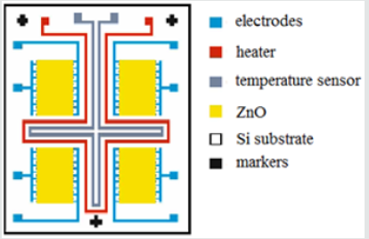
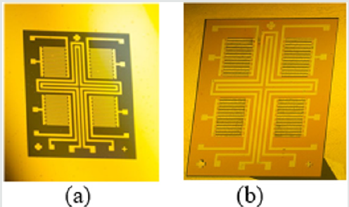
For the sensor fabrication, a surface micromachining technology, with several step of layer deposition and striping of constructive and sacrificial layers, is used. This technology is needed for structuring of the sensitive layer and the metal interdigitated electrodes used as integrated heater and temperature sensor. For the produced ammonia sensor, working in resistive mode, the resistance between electrodes and gas sensitive film of ZnO is changed, as a result of the contact with ammonia. In (Figure 1), a structure of the interdigitated electrodes, deposited on silicon substrate, with metal-oxide sensitive layer of ZnO is presented. The structure contains four independent sensors areas, situated on common substrate. The heater and the temperature sensor are platinum films grown between them, in order to support of constant temperature and measure the thermal field change during the process of sensor testing and operation.
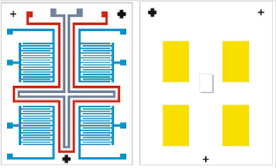
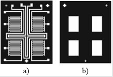
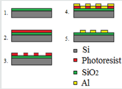
The integrating of the heater and temperature sensor additionally complicates the manufacturing process when aluminium is used for electrodes, because of the increased number of photolithography steps. However, if a platinum is used as a metal layer, for producing of the heater, temperature sensor and electrodes, the technological process will include only two additional photolithography steps, but there will be a limitation in the film thickness, and, as a result, in the resistance and the power of the heater. In (Figure 2) layers of the sensor are presented. This sensor consists of two main layers - platinum and zinc oxide, which are structured by inverse photolithography. The using of the lift-off process, instead of standard photolithography, is preferred, because, in this case, the etching process of metal electrodes and sensitive layer is avoided, preventing the influence on the previously deposited film and destroying them. In (Figure 3), the photomasks for the both lift-off processes are shown. The thermally oxidized silicon wafer is used as a substrate. The thickness of the silicon oxide is 100nm, which is necessary for dielectric isolation between the metal electrodes, heater, temperature sensor and substrate. The technology sequence is shown in (Figure 4). As a “sacrificial” layer, the positive photoresist AZ1350 is used. The negative topology image of electrodes is formed by the first photomask. On the top, a 150nm platinum film is deposited by sputtering. After stripping of the “sacrificial” layer, only structured comb electrodes remain on the top. By using the second photomask, the next “sacrificial” layer is formed, defining the topology of the sensitive layer only on the electrode’s areas, as shown in (Figure 5). For the deposition of thin ZnO layer, the sputtering targets of ZnO, with a purity of 99.99% was purchased from “Goodfellow”, respectively with 75mm diameter and 3mm thick. ZnO target was mounted in vacuum chamber of Leybold sputter coating system A400 VL. The film was deposited by RF sputtering process. The exact deposition conditions were as follow: base vacuum 2x10⁻⁵Torr, the sputtering argon gas 2.5x10⁻²Torr, sputtering voltage Uplsm = 0.75kV, Iplsm = 150mA, sputtering power Pplsm=112W. The growth rate was 9 nm/min ZnO. The thickness of ZnO layer was 250 nm.Each one of the pair electrodes includes 16 fingers, having width and distance between them, of 120µm, respectively.
Results and Discussion
Ammonia NH3 Source
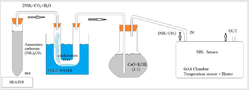
The produced sensor structures were tested and calibrated in laboratory conditions. By this reason, it was necessary, during the measurements to provide constant ammonia flow. In the most frequently cases, this is realized by using of pure ammonia source with an adjusting system for regulating gas flow through the chamber. The similar unit required complex equipment that makes the measurement more expensive. For this reason, in this case, in order to provide a constant ammonia flow during measurements, a thermal reduction of ammonium carbonate, at 7˚С was used. During this reaction, some quantities of NH3 and CO2 were obtained. The disposition of the experimental arrangement is shown in (Figure 6).
((NH4)2CO3) → NH4HCO3+NH3 → 2NH3+CO2+H2O(1)
After thermal reduction and passing through a dryer, the mixture of 66% NH3 and 33% CO2enters into the chamber. That ratio remains constant until the source is heating. The chemical reaction can be quantitatively submitted as:
NH4HCO3→2NH3+CO2+H2O (2)
9,63,44,41,8 [g/mol]
Testing and Calibration
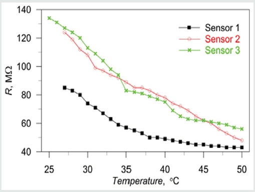
All 4 sensors from the structure were tested simultaneously in one cycle. In such case, the received data can be averaged, decreasing the measuring error. The measuring temperatures were changed in the range 25-50 ˚С with a step of 1˚С with a changing speed of 1˚С per minute. The results from the measurements are shown in (Figure 7), where 3 of the 4 segments showed reliable results. From the curves, is could be estimated the excellence linearity of the sensor’s response during the NH3 flow exposure. With the increase of the temperature, the resistance of the sensors is reduced. The response time (not shown) is approximately 30ms, but the recovery time is longer - about 1 min-due to the lower temperature at which desorbing process should occur. By the authors knowledge, these times are improved as compared to similar low-cost solution, which can be attributed to the newly proposed heater design. The resistance of the sensor 1 is lower than the others, due to shortening of some interdigitated segment electrodes.
Conclusion
The ammonia sensor was produced by surface MEMS technology. ZnO was used as a gas sensitive layer. It was estimated by applying resistive measuring principle. The realized sensor is from the group of low temperature type MOx chemical sensors, suitable for using near the room temperature operation range. The temperature dependence of the sensors response and sensors recovery time was shown to be satisfactory. A simple method for providing of ammonia gas is proposed, which is necessary for testing and calibration of the structure. The future work will be done in the direction of defining of the sensor selectivity, increasing its response time, as well as its possible integration in micro chemical lab and MEMS devices for environment control.
Acknowledgement
This paper was presented at INERA Conference „Vapor Phase Technologies for Metal Oxide and Carbon Nanostructures “, 5-9 July 2016, Velingrad, Bulgaria. The Conference is part of the Program of INERA REGPOT Project of Institute of Solid-State Physics, Bulgarian Academy of Sciences.
References
- Wang C, Yin L, Zhang L, Xiang D, Gao R (2010) Metal oxide gas sensors: sensitivity and influencing factors. Sensors 10(3): 2088-2106.
- Hyojin K, Le Hung N, Eunseong A, Jung H, Dojin K (2010) Synthesis and Gas Sensing Properties of ZnO Nanostructures. J of the Korean Physical Society57: 1784-1788.
- Pandya H, Chandra S, Vyas A (2011)SENSORDEVICESThe Second International Conference on Sensor Device Technologies and Applications, India.
- Suchea M, Christoulakis S, Moschovis K, Katsarakis N, Kiriakidis G (2006)ZnO transparent thin films for gas sensor applications. Thin Solid Films 515: 551-554.
- Dighavkar C(2013)Characterization of nanosized zinc oxide based ammonia gas sensor.
- Janotti A, Walle C (2009) Fundamentals of zinc oxide as a semiconductor. Rep Prog Phys72:
Archives Appl. Sci Research5(6):96-102.

Top Editors
-

Mark E Smith
Bio chemistry
University of Texas Medical Branch, USA -

Lawrence A Presley
Department of Criminal Justice
Liberty University, USA -

Thomas W Miller
Department of Psychiatry
University of Kentucky, USA -

Gjumrakch Aliev
Department of Medicine
Gally International Biomedical Research & Consulting LLC, USA -

Christopher Bryant
Department of Urbanisation and Agricultural
Montreal university, USA -

Robert William Frare
Oral & Maxillofacial Pathology
New York University, USA -

Rudolph Modesto Navari
Gastroenterology and Hepatology
University of Alabama, UK -

Andrew Hague
Department of Medicine
Universities of Bradford, UK -

George Gregory Buttigieg
Maltese College of Obstetrics and Gynaecology, Europe -

Chen-Hsiung Yeh
Oncology
Circulogene Theranostics, England -
.png)
Emilio Bucio-Carrillo
Radiation Chemistry
National University of Mexico, USA -
.jpg)
Casey J Grenier
Analytical Chemistry
Wentworth Institute of Technology, USA -
Hany Atalah
Minimally Invasive Surgery
Mercer University school of Medicine, USA -

Abu-Hussein Muhamad
Pediatric Dentistry
University of Athens , Greece

The annual scholar awards from Lupine Publishers honor a selected number Read More...


