Lupine Publishers Group
Lupine Publishers
Menu
Review ArticleOpen Access 
Nanowires: Synthesis, Applications and Challenges Volume 1 - Issue 3
Billel Salhi*
- Center of Research Excellence in Desalination and Water Treatment, King Fahd University of Petroleum& Minerals, Dhahran 31261, Saudi Arabia
Received: October 12, 2020 Published: December 09, 2020
Corresponding author: Billel Salhi, Center of Research Excellence in Desalination and Water Treatment, King Fahd University of Petroleum& Minerals, Dhahran, Saudi Arabia
DOI: 10.32474/JBRS.2020.01.000112
Abstract
In this Review, I report an update on the with special attention given to silicon nanowires and SiGe. The flap on the different techniques of characterization of the nanowires and the potential applications of nanowires was also discussed. Several methods are explained to fabricate the semiconductor nanowires and particularly the silicon nanowires. The technique VLS (Vapor Liquid Solid) proves to be the most used technique and adapted for the synthesis of nanowires with high efficiency. Silicon nanowires have shown great potential for the realization of new devices for electronics (field effect transistors), diodes, displays, photovoltaic, energy storage, thermoelectricity, biotechnology. Some of its applications nanowires are not currently an industrial product. If the methods of elaboration are numerous, they do not yet combine the mass production and the very small dimensions. The set of physical phenomena observed is not explained or perfectly understood as, for example, the phenomena of electrical conduction, thermal, mechanical, optical and magnetic properties. The stakes are important and the control of the nano-object and the nanowire in particular is crucial
Keywords: Nanowires; thermoelectric; photovoltaic
Introduction
Nanowires are structures of dimensions of the order of one nanometer (10-9m). Alternatively, they can be defined as structures that have a lateral size of a few tens of nanometers or less and a longitudinal size without limit. At these scales, the quantum mechanical effects are important, therefore such wire are also known as "quantum wires". Many different types of nanowires exist, metallic (Ni, Au, Pt...), semiconductors (InP, Si, GaN, etc.), and insulators (SiO2, TiO2). Molecular nanowires consist of a repetition of organic (DNA) or inorganic molecular units (Mo6S9-xIx). Nanowires have received special interest due to their applications in electronic and optoelectronic devices. Many applications at room temperature have already been shown, such as field effect transistors (FETS) [1], diodes [2], and logic gates [3] combining n-type and p-type nanowires. In addition, it has been shown that it is possible to obtain the almost atomic pointed interfaces between InAs and INP [4]. From a fundamental point of view, nanowires are an excellent sample for the study of one-dimensional systems. Low dimensional systems are of great interest because dimension plays an important role in determining the properties of the material. For example, electrons act differently in 3D, 2D, 1D and 0D structures, which affect the gap of materials, the density of states, the effective mass of electrons or holes.
Interest of nanowires
The first 1D nanostructure to be synthesized are carbon nanotubes, discovered by Iijima in 1991 [5]. Following this first discovery, the researchers were interested in the synthesis and characterization of other 1D structure, which include nanos, nanobonds and nanoribbons. Inorganic nanos can play the role of active components in electronic systems, as recent studies have shown [6]. As we have already mentioned, the modular and unusual properties of these nanostructures make it possible to integrate them into vast application domains such as electronics, optics, heat, photovoltaics, biology, chemistry, and mechanics. We are particularly interested in applications in microsources of energy, in particular in thermoelectricity and photovoltaics, as well as in electronics applications.
Interest of nanowires for thermoelectricity
Conventional refrigeration systems using compressionrelaxation cycles include moving parts, sources of vibration and noise. On the contrary, the thermoelectricity is based on the direct conversion of the thermal energy into electrical energy via physics phenomena of the solid. The thermoelectric converters do not have moving parts. The absence of vibration makes it possible to consider their use for applications where the vibrations are considerably annoying as in the laser guidance systems or the integrated circuits. They are easier to use and more compact. However, converter yields currently marketed are of the order of 10% which remains low compared to 30% of vapor compression refrigerators. The manufacture of these new small-size thermoelectric converters will help cool the electronics,but will also produce electricity from energy lost by e and joule. The integration of nanostructures such as nano ls into these converters will allow an unprecedented increase in efficiency [7].
Both applications
Thermoelectric refrigeration: this is the creation of a heat
unit that opposes the heat dissipation, when a material subjected
to a thermal gradient is traversed by a current I [8]. Electrical
Generation: This is the conversion of a heat unit into an electric
current. In particular, heat can be supplied from lost heat sources,
such as automobile exhaust pipes, incinerator chimneys, and
nuclear power plant cooling circuits.
Three thermoelectric effects have been
observed on a material:
the e and Seebeck, the e and Peltier and the effect Thomson. These
are volume effects, not surface effects [9]. These three effects are
linked by simple relationships described by the Onsager equations
of the name of the physicist who made them explicit. Each e is
associated with a coefficient of its own. Thus the knowledge
of the evolution of only one of these coefficients as a function of
temperature, T, makes it possible to deduce the two others [10].
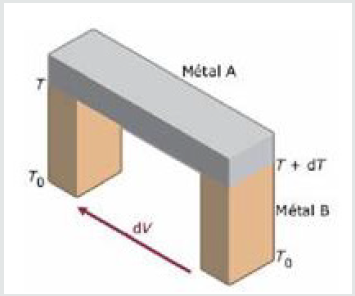
The Seebeck effect: The Seebeck effect was discovered in 1821
by Thomas Johann Seebeck. When a junction of two different
materials A and B is subjected to a temperature gradient T, the result
of this same junction is the appearance of an electromotive force
(f.e.m.) as schematized on Figure 1 Physically, the Seebeck effect can
be explained by the polarization of any conductive element placed
in a temperature zone where the gradient is non-zero. Conduction
electrons are observed from the hottest end to the coldest end.
Their speed depends on the temperature. Since hot electrons are
faster than cold electrons, the hot end is positively charged and the
cold end negatively. An electric field is born and the latter, according
to the law of Heinrich Lenz, opposes the electronic movement that
gives birth to it. This field, which depends on the characteristics of
the materials and, in particular, the thermoelectric power, is at the
origin of the so-called Seebeck voltage. The hot electrons are then
slowed by the internal electric field created and the cold electrons
are accelerated. A dynamic equilibrium is established: the diffusion
of the hot electrons is compensated for by the diffusion of the cold
electrons. A conductive material element of a certain length can,
therefore, be assimilated to an elementary voltage generator [9].
The Peltier effect
The Peltier effect is the release or absorption of heat, other than the Joule effect, caused by the passage of an electric current through the junctions of two conductors A and B at the same temperature. This effect discovered in 1834 by Jean-Charles Athanase Peltier involves an exchange of very small quantities of heat. This exchange is proportional to the intensity of the electric current I in the circuit and depends on the temperature at which the system is located [9].
Example of Si/SiGe nanowires in thermoelectricity
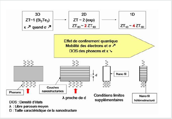
As mentioned above, the nanostructures have properties quite different from the bulk material of the same composition. In the field of thermoelectricity, the aim of technological research is twofold: to seek to improve conversion efficiency by using low-dimensional structures, while benefiting from mass production systems. The study of low dimensional structures has become very important since improvements Notable factors of the ZT merit factor were predicted theoretically and then observed experimentally. The optimization of phonon dynamics and heat transport physics in nanostructured systems has yielded promising results [11-12]. Nanostructures must be prepared with one or more dimensions less than the average free path of phonons and greater than that of electrons and holes. This would potentially reduce thermal conductivity without decreasing electrical conductivity [13]. (Figure 2) illustrates schematically the reduction of the ZT when the dimension is reduced and the nanostructuration increases.
Two main effects affect the thermoelectric properties of the material when it is nanostructured. The first effect is a strong diffusion of phonons by the grain boundaries (boundaries between the different grains constituting the material) and by the edge effects (roughness of the surface of the material) inducing a decrease of thermal conductivity of network. The second appears in the form of quantum-type quantum conduction effects of charge carriers that strongly modify the properties of electrical transport (electrical conductivity and coeficient). Seebeck). Very high values of the ZT merit factor, of the order of 2.5 at room temperature, have thus been observed in the laboratory in stacking structures. Thin layers of nanometric order. At present, these structures are mainly envisaged for applications at low or medium temperatures (<150-200 C). One of the main difficulties is, in fact, to obtain thin thermoelectric layers whose properties do not decay when the temperature increases [8].
The most widely used thermoelectric material is Bi2Te3 bismuth tellurium and its alloys with antimony Sb and Serium Se, among others, which have a ZT close to 1. It is difficult to transfer the massive Bi2Te3 for energy conversion on a large scale. In addition, making nanostructures for this purpose is even more difficult. These materials also have the disadvantage of being very toxic to the environment. Silicon, on the other hand, is the most abundant semiconductor on earth and widely used in the microelectronics industry. However, solid silicon has a high thermal conductivity (≈ 150 W.m-1.K-1 at room temperature [15] which gives a ZT≈ 0.01 to at 300K [16]. Since the crystalline structure of silicon nanoids is similar to that of solid silicon, it is necessary that nano-induced size changes have a strong influence on phonon physics and conductivity. Thermal to improve the value of the ZT.
Phonon physics is important for silicon nanowires in which the structure of silicon is similar to that of solid material [17]. The spectral distribution of the phonons contributing to the thermal conductivity κ is relatively broad. It is necessary to distinguish phonons from weak, medium and high frequencies. The point defects mainly cause the diffusion of phonons of high frequencies. The Umklapp broadcast allows those of medium frequencies. Indeed, the diffusion by phonon-phonon Umklapp mechanism is proportional to ω2, where ω is the phonon frequency so it remains weak as long as the phonon frequency remains low. It is the low frequency acoustic phonons that contribute significantly to the conduction of heat and thus to the value of κ at high temperature [18-19]. Phonons at low frequencies are mainly affected by diffusion at the interfaces, hence the interest of nanostructuration. Another method used to reduce thermal conductivity is the rational incorporation of phonon dielectric elements at different wavelength scales. Thanks to these different means of action, the thermal conductivity κ should decrease considerably.
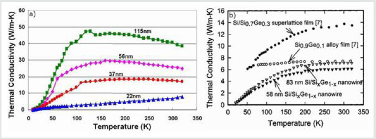
Since 2000, experimental values of ZT up to 2.4 with supernetworks have been obtained [11]. When used as a cooler, a study has shown that a material developed in a superlattice (ex. Si / SiGe) makes it possible to obtain a greater temperature difference than the alloy material of the same kind (ex. SiGe). The ZT, theoretically estimated at 2, was measured in the range 1.3-1.6. This improvement with respect to the merit factor obtained with solid materials is attributed largely to the structuring of the material [21]. Thermal conductivity measurements have been made on superstructures and isolated nanowires [8,20]. According to the literature, only a single measurement of thermal conductivity on Si / SiGe nanowires has been published [22]. As shown in Figure3a, single-crystal silicon nanowires have a thermal conductivity that varies with the diameter of the nanowire. The smaller the diameter, the lower the thermal conductivity. A 115 nm diameter wire has a thermal conductivity of 45 W/m.K at room temperature (273K), while a 22 nm wire has a thermal conductivity of 5 W /m.K, which is nine times more low. For this reason, one of the objectives of the thesis will be to synthesize nanowires of small diameter.
The heterostructured Si/SiGe nanowires are very interesting
for thermoelectricity because of their low thermal conductivity.
Figure2b shows that heterostructured Si/SiGe nanowires have
a lower thermal conductivity than Si/SiGe super networks. For
equivalent diameters, they also have a thermal conductivity lower
than that of simple silicon nanowires. The thermal conductivity of
a silicon nanowire of 115 nm in diameter is 45 W/m.K, which is
three times higher than that of a Si /Si07 Ge 0.3 superlattice with
a thermal conductivity of 14 W / m.K. Whereas that of a Si/SiGe
nanowire 83 nm in diameter is 7 W / m.K, which is twice as small
as that of the Si / Si0.7Ge0.3 superlattice. For the same diameter
of nanowire (56 nm in Figure 2a and 58 nm in Figure 3b), a
heterostructured Six/SiGe1- x nanowire has a thermal conductivity
(6 W/m.K) five times lower that of a single nanowire (30 W / m.K),
which proves the effect of structuring on the reduction of thermal
conductivity. According to the literature, measurements have not
been published for Si/SiGe nanowires with a diameter smaller than
58 nm.
On the other hand, a recent study took place on nanowires
realized by CVD and by electrochemical etching exhibiting a strong
surface roughness. It has been shown that the thermal conductivity
can be decreased up to ∼1.6 W / m•K with a phonon contribution
close to that of the limit of amorphous material. Thus a ZT = 0.6
at room temperature has been obtained without significantly
modifying the power factor S2/ρ (remember that σ=1/ρ). (Figure
3) shows the measurement system of a nanowire as well as
the different tracers obtained from κ for different diameters of
nanowires and the tracés of ρ, S, κ bulk /κ nw , (S2 /ρ) bulk /(S2
/ρ)nw , S2 /ρ and finally ZT.
Figure 3: Evolution of thermal conductivity as a function of temperature a) for different diameters of monocrystalline silicon nanowires and b) for Si / SiGe super networks and for two Si / SiGe nanowires [8, 20].
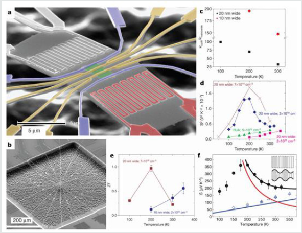
Recently, a team has gone further in thermoelectric measurements on insulated etched nanowires. A device suspended in the vacuum, shown in Figure 4 (SEM image a and b), made it possible to obtain measurements of thermal and electrical conductivities, Seebeck coefficient S and thus to deduce a value of ZT. The vacuum suspension limits the interface contact resistances and increases the reliability of the results. The image in (Figure 3b) shows the system wiring that is suspended in the center. It should be noted that the measured nanowires are not round nanowires synthesized by the bottom-up pathway but rectangular section nanowires synthesized by the top-down pathway by means of a pattern transfer method (patterning) [23] . (Figure 4c)shows the evolution of the thermal conductivity for nanowires which all have a height of 20 nm and widths of 20 nm (black dots) or 10 nm (red). The κbulk / κnanowire plot highlights the decrease of κ involved in the value of the ZT. (Figure 3d) shows S2 as a function of temperature for nanowires of section 20 nm x 20 nm. The most doped nanowires behave similarly to the weaker doped solid silicon. For nanowires at slightly lower and slightly higher concentrations, S has a peak around 200K. This is a consequence of the one-dimensional nature of silicon nanowires. (Figure 4e) gives the value of ZT as a function of temperature for doped nanowires of 20 nm x 20 nm. A maximum ZT of 1 is obtained at 200 K for the nanowire 20 nm wide. The difference between the two types of wires is explained by the fact that, for the nanowire 20 nm wide, the thermoelectric S is dominated by the contribution of the phonons whereas, for the nanowire 10 nm wide, it is dominated by electronic contributions. This is verified on the plots of Figure 3f. In black is drawn the theoretical expression of S where S = Se + Sph. The red curve corresponds to the contribution of the phonons Sph and the blue curve to the contribution of the electrons S. The blue dots are experimental ph measurements from wide wires (520 nm x 35 nm, doped 2.1020 at.cm-3, blue crosses), 10 nm wide wires (doped at 7.1019 at.cm-3, diamonds blue) and strongly doped 20 nm wires (1.3.1020 at.cm-3, blue triangles). The electronic contribution, linear according to the temperature, is found thanks to the approximation between the points and the blue curve. The insertion of the phonon contribution is found for the black dots corresponding to the nanowires of 20 nm wide doped at 3.1019 at cm-3 and where we see that the theoretical curve is very close to the points [17].
Figure 4: (a-b) SEM images of the suspended device of thermoelectric measurements of etched Si nanowires. (c-f) The theoretical and experimental κbulk /κnanwire, S2, ZT and S plot [17].
These first ZT values obtained with silicon nanowires are promising. With optimized doping, diameter reduction and roughness control, the value of ZT will most likely increase. This is already proven at the level of the decrease in thermal conductivity. In short, for the Si/SiGe nanowires to be a good thermoelectric material, it is necessary initially to be heterostructured, of small diameter, and of a sufficient length in order to be able to integrate them in the thermogenerator.
Interest of nanowires for photovoltaics
Solar cells are promising systems for generating clean,
renewable energy. With miniaturization, solar cells can also be
integrated as microsources of energy in nanoelectronic systems.
The use of nanostructures or nanostructured materials represents
a general approach to reduce both cost and size and to improve
photovoltaic efficiency [24]. To be effective, solar cells must meet
two criteria. First, they need to absorb light, so they need an active
material that is thick enough to have maximum absorption. They
also need to collect electrons from the electron-hole pairs created
by the absorbed photons. Fine material is generally better because it
limits the trapping of electrons in the material. One of the solutions
to reconcile these constraints is to make relatively thin layers and
use extremely pure and crystalline materials which eliminates
impurities and defects likely to trap electrons. Such materials
give good results but are very expensive which makes the price of
solar panels high. Nanowires offer an interesting alternative. On
the one hand, nanowires can absorb large amounts of light along
their length. On the other hand, the advantage of nanowires is to
reduce the distance that exists between the n-p junction and the
electron collector. Some devices have been developed [24-27] and
two main configurations have emerged. The first configuration is to
synthesize the complete device around the nanowire through radial
layers as shown in (Figure 5) [24]. Thus, the electrons travel a very
small distance before being collected simply by passing through
the so-called shell layer. As the layers are thin, the risk of electrons
being trapped is low, so it is possible to use cheaper materials with
more defects [27].
(Figure 5) (a-d) Photovoltaic device based on a coaxial
nanowire p-i-n. Scheme (a-b) and MET (c-d) image of the nanowire
device and structure [24]. (e) Device based on a nanowire forest
covered with amorphous silicon and SEM image of the nanowire
carpet seen from above, in section and in zoom [25]
Figure 5: (a-d) Photovoltaic device based on a coaxial nanowire p-i-n. Scheme (a-b) and MET (c-d) image of the nanowire device and structure [24]. (e) Device based on a nanowire forest covered with amorphous silicon and SEM image of the nanowire carpet seen from above, in section and in zoom [25].
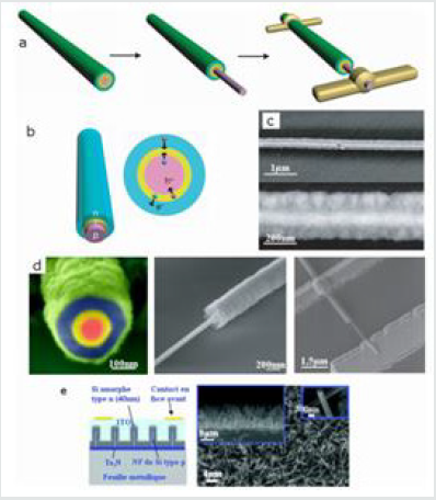
The second configuration is to use as a base a nanowire forest. The junction np is obtained in two ways: either the substrate is p-doped and the n-doped nanowies [26], or the nanowires which are p-type are coated with a conformal deposit of amorphous silicon of the n-type [25] as shown in (Figure 5); which gives in both cases an n-p junction. The production of electricity from these cells has been validated but a long way remains to be done before commercialization. For large-scale applications, it is necessary to grow dense forests of nanowires. Moreover, the biggest current limitation is the low efficiency of these photovoltaic cells. For example, on a single wire, a yield of only 3.9% of incident light in electricity was obtained, which is still far from the almost 20% achieved with conventional solar panels. The objective of increasing the efficiency of these solar cells is to obtain denser nanowire mats, to reduce the contact resistances, to minimize the diffusion, to optimize the geometry of the nanowires (diameter distribution, orientation properties ...) and improve the quality of the np junction [25,27].
Nanowires and biotechnology
Nanowires and other materials are potentially extremely interesting objects for nanobiotechnologies. They have particular electrical characteristics that can be disturbed by chemical reactions on their surface between target molecules to be detected and probes attached to the surface of the nanowire. The detection and measurement of these effects makes them detectors both sensitive, not requiring marking, and fully integrable (the sensitive device processing electronics) on a chip. This makes them extremely serious competitors to methods commonly used today [8]. Today, the main issues concern the improvement of performance in terms of sensitivity, the integration of complete and “multiplexed” detectors (several detections in parallel like DNA or prote in chips), as well as the at the point of competitive manufacturing processes from an industrial point of view.
Types of nanowires
Since the early 2000s, nanowires of various inorganic materials have been synthesized and characterized. Recall that when we speak of nanowires, it is cylinders full of tens of nanometers in diameter (typically 1-100 nm) and length that can go up to several hundred microns. The nanowires can be organic, metallic or inorganic (oxides or non-oxides), mono or polycrystalline. Thus, nanowires of single elements (Si, Ge, SiGe, Si / SiGe), oxides (TiO), nitrides (BN), carbides (SiC) and chalcogenides 2 (CdSe) have been produced. One of the crucial factors in the growth of nanowires is the control of composition, geometry and crystallinity [6].
Nanowires synthesis methods
The literature which deals with the synthesis and the study of the physico-chemical properties of nanostructures and in particular nanowires is rich and abundant. A large number of growth techniques are referenced. However, there is often confusion between the growth mechanism (VLS, SLS, VS.) and the experimental method of synthesis (CVD, laser ablation ...). In many cases, the growth mechanism has not yet been clearly established. And there are many contradictions that can appear in the results and / or their interpretations. The methods of synthesis can be classified in two ways. The first is to separate the so-called physical methods from the so-called chemical methods. Physical methods involve patterning, lithography, template and electrofilming techniques. Lithography and pattern techniques are top-down approaches while electro-casting and mussel techniques are bottom-up approaches. Chemical methods include precursor decomposition (LS, SLS, VS and VLS), oxide assisted growth, solvothermic, hydrothermal, carbothermic and electrochemical methods. The second classification that which we will follow, separates the techniques in vapor phase of the techniques in solution. Some chemical techniques will only be possible if there is solubility or even eutectic between the catalyst and the nanowire material. This is the case for the vapor-liquid-solid process (VLS) which, therefore, cannot be applied to all materials[6].
Growth of nanowires in solution
The Liquid-Solid Mechanism (LS):
owth by LS mechanism is possible for materials with strong bond anisotropy, which promotes crystallization along the c-axis. This is the case for sulphide polynitride, (SN)x selenium [29], tellurium [30] and molybdenum chalcogenides [31, 32]. This technique allows the selective growth of nanowires with a very low density of structural defects and high purity but has the disadvantage of non-localized growth.
The solid-liquid-solid (SLS) mechanism
The solid-liquid-solid (SLS) and vapor-liquid-solid (VLS) mechanisms are catalytic growth mechanisms. Based on an analogy with the VLS mechanism, the SLS mechanism was developed to achieve faster growth rates than the VLS mechanism and for lower temperatures [33]. By this method, Group III-V semiconductor crystalline nanowires [34, 35, 36] have been produced. The diagram in Figure 1.15 clearly shows the growth of nanowires or nanowhiskers by the SLS method. The products obtained are generally monocrystalline with dimensions of 10 to 150 nm in diameter and length greater than several microns. The Supercritical Fluid-Solid-Liquid (SFLS) method, where a supercritical fluid replaces the solvent, has been used to generate large amounts of silicon and germanium nanowires without and monocrystalline [37, 38]. Nanowires 4-5 nm in diameter and longer than several microns have been synthesized. The key to this synthesis is the use of gold nanocrystals, monodisperse and encapsulated in an alkanethiol, which serve as seeds for a direct and confined growth creating silicon nanowires with a Narrow size distribution. In a classical procedure, the statically stabilized gold nanocrystals and the Si precursor, diphenylsilane, are co-dispersed in hexane which is heated and pressurized beyond its critical point. Under these conditions, diphenylsilane can decompose to form Si atoms. The Au-Si phase diagram indicates that silicon and gold can form an alloy in equilibrium with pure silicon. when the concentration of silicon relative to gold is greater than 18.6 mol- % and the temperature is higher than 363 C. Thus, the atoms of Si dissolve in gold nanocrystals until saturation. At this point, the atoms are rejected from the alloy and form a uniform nanowire. This mechanism is similar on many points of the SLS mechanism. The supercritical fluid is necessary to be in the conditions that will allow the dissolution and crystallization of silicon. More interesting, the orientation of Si nanowires can be controlled by adjusting the pressure [28, 6, 40,39].
Solventothermic reactions
The solvothermic pathway is much used to realize semiconductor nanowires. The major advantage of this approach is that most materials can be soluble in a suitable solvent by heating and pressurizing the closed system to near its critical point. Thus, this approach is available for many solid materials. This method is versatile and has enabled the growth of various semiconductor nanometers [41, 42], nanotubes [43-44] and whiskers [45, 46]. However, the products are characterized by low yield, low purity and poor uniformity in size and morphology [6, 40].
Growth from a mold (template)
There are two types of molding techniques (templating): chemical molding and physical molding. The chemical molding can be based on a hard mold (‘hard templating’) or a ‘soft’ mold, that is to say in solution (‘soft templating’), while the physical molding is always based on a mold hard. Template growth is an easy and flexible way to generate 1D nanostructures. The nanomaterial will be made around or inside the mold: there is a direct correlation between the morphology of the mold and that of the nanostructures. We present only one type of chemical molding and one type of physical molding.
Soft Templating Mold
Self-assembled structures from surfactants (Figure 6)
provide a useful and flexible class of molds for the generation of
1D nanostructures in large quantities. Above the critical micellar
concentration, the surfactant molecules spontaneously organize into
micelles with rod shapes [40, 47]. Based on this method, nanowires
of CuS, CuSe, CdS, CdSe, ZnS and ZnSe were made using surfactants
such as Na-AOT (sodium dis2-ethyl-hexylsulfosuccinate) or Triton
X-100 [48, 49].
Physical mold from a porous membrane: The molds can be
nanoscale channels with mesoporous materials, porous alumina
or polycarbonate membranes [50-53]. The nanoscale channels
are filled with a solution, a sol-gel or an electrochemical method. The nanowires thus produced are separated from the mold by
removing the latter. Two types of porous membranes are frequently
used: polycarbonate and alumina. For polycarbonate membranes,
a polymer layer (6-20 mm) is irradiated with heavy ions to induce
holes on the surface of the layer. These holes are then developed by
chemical etching to generate uniform cylindrical pores through the
layer of polymer. Pores made using this method are often randomly
distributed on the surface of the polymer membrane. They can also
be inclined more than 34° relative to the surface [54]. In contrast to
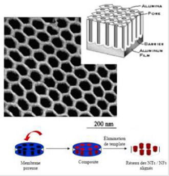
chemically etched polymer membranes, the alumina membrane is
prepared by anodizing an aluminum foil in a medium acid (Figure
7)[55]. Many materials have been synthesized as nanowires using
porous alumina membranes as a mold: Si [56], Au, Ag, Pt, TiO2,
MnO2, ZnO, SnO2, In2O3, CdS, CdSe, CdTe, conductive polymers
such as polypyrole, poly (3-methylthiophenene) and polyaniline
and also carbon nanotubes. In contrast to polymer membranes,
the pores of the alumina membrane are only slightly or not at all
inclined relative to the surface of the membrane and their density
is much higher. This method must, in general, be coupled with
another one, whether it is chemical (electroplating [57, 58], sol-gel)
or physical (catalyst deposition at the bottom and then CVD [59,
60], for example) to deposit the catalyst at the bottom of the holes.
In addition, it is difficult to obtain monocrystalline materials by this
method. The advantages of physical molding is to be able to make
nanostructures with complex or amorphous phases and to have a
control of the geometry of structures through that of the mold. The
cost of manufacturing by this method is more competitive than that
described above, using nanowires or nanotubes as a mold. Another
advantage of this method is that it is possible to obtain networks
of aligned 1D nanostructures, which can be very interesting for
certain applications [28, 6].
Figure 6: Schematic of the formation of nanowires from surfactant molecules. a) formation of the cylindrical micelle, b) formation of the nanostructure desired, c) removal of the surfactant with a solvent or by calcination to obtain the individual nanos [40].

Figure 7: Schematic and MET image of a nanoporous alumina membrane [50] and general principle of physical templating from the pore network of a membrane [28].
Growth of nanowires in the gas phase
The growth of nanowires from the gas phase is probably the most explored approach for the synthesis of whiskers and nanowires. It includes the following techniques: evaporation in an atmosphere suitable for producing elementary nanowires or oxides, the vapor-liquid-solid technique (VLS) and the vapor-solid technique (VS) [6, 40]. Oxide-assisted growth: Among the growth mechanisms of nanowires, the oxide-assisted growth mechanism has been proposed. There is no need for a metal catalyst for this type of growth. The growth of silicon nanowires is possible thanks to silica powder targets containing silica [61-65]. The quantities obtained are of the order of a few milligrams, which is much higher than what is obtained by CVD (a few micrograms). In this case, the SixO vapor generated by thermal evaporation or laser ablation has a key role in oxide-assisted growth. The nucleation that takes place on the substrate occurs according to the following reactions:
SixO →Si +SiO (x > 1) (1)
2SiO →Si +SiO2 (2)
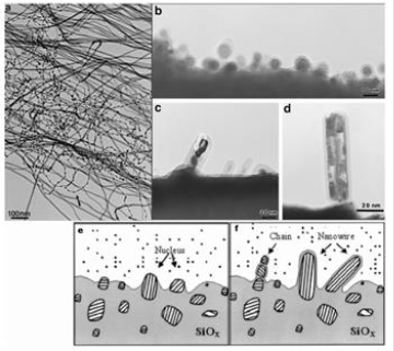
The decomposition reactions described in (1) and (2) result in the precipitation of silicon particles which will act as nuclei of the silicon oxide coated silicon nanowires. Precipitation, nucleation, and growth occur near a cold zone of the substrate, suggesting that the thermal gradient provides the driving force for nanowire formation and growth. (Figure 8) (a, b, c and d) shows the MET images of the early stages of nanowire formation. In Figure a, the silicon nuclei are coated with amorphous silicon. The tip of nanowires contains many structural defects. (Figure 8) (e and f) shows a diagram of the growth mechanism. The growth of silicon nanowires is determined by three factors:
a) The catalytic effect of the SixO layer (x <1) on the tips of
the nanowires.
b) Braking of lateral growth by the presence of SiO2 in the
outer layer of the nanowires formed by the decomposition of SiO.
c) Stacking faults along the direction of growth <112> of the
wire
It has been noted that only nanowires having their direction of growth parallel to the direction <112> grow rapidly (Figure 8). This method makes it possible to obtain inter alia nanowires with very small diameters, between 1.3 and 7 nm [65]. By this oxideassisted growth method, nanowires of Cu2S [66], CuO [67] and MgO [68] have also been synthesized. The major advantage of these oxide-assisted methods is that there is no need for a metal catalyst and, as a result, contamination by the metal atoms of the catalyst is eliminated. Another advantage is the decrease of the growth temperature, which has been observed for the synthesis of MgO [6, 68, 40].
Figure 8: MET (a) images of Si nanofils obtained by oxide assisted growth, (b) silicon nuclei at the beginning of growth and (c-d) nanowires at the beginning of growth. (e-f) Scheme of growth with formation of silicon oxide matrix, then formation of silicon nuclei and growth of nanowires [61].
The vapor-solid mechanism (VS):
As for the liquid-solid method (LS), when a solid has an anisotropic crystallographic structure or a preferred growth direction, it is possible to grow nanofis from the gas phase: this is the vapor-solid method (VS). In this process, evaporation, chemical reduction or gaseous reaction generate the vapor. The vapor is transported and condensed on the substrate which is placed at a lower temperature than the source material. Experimental techniques exploiting this process are numerous: CVD (chemical vapor deposition), HFCVD (chemical vapor deposition assisted by a hot filament), MOCVD (chemical vapor deposition from organometallic precursors), laser ablation, evaporation thermal, etc. [40, 69]. The vapor-solid method has been used to synthesize oxide whiskers as much as metals with diameters in the micron range. By this method, nanowires of some metal oxides have been obtained such as Si3N4, SiC, Ga2O3 and ZnO by heating the commercial powders of these elements at high temperature [6, 70]. This method also makes it possible to produce original structures such as nanoribbons by controlling the nucleation / growth conditions (Figure 9). The advantages of this process are to obtain very pure nanowires chemically by a vapor phase method, which is simple and accessible, thanks to the use of simple experimental systems.
A. Carbothermic reactions:
Nanowires of oxides, nitrides and carbides can be synthesized by carbothermic reactions. For example, carbon mixed with a metal oxide produces a suboxide or metal species in vapor form. These species react with carbon, oxygen, nitrogen or ammonia to produce GaN nanowires. MgO nanowires were also produced by this method. Depending on the desired product, the sub-oxide heated in the presence of oxygen, ammonia, nitrogen or carbon will produce nanowires of oxide, nitride or carbide [6]. Hydrogen or water can also be used as a reducing agent. And this method can also be extended to binary oxides such as Al2O3, ZnO and SnO2[40].
The vapor-liquid-solid mechanism (VLS)
Among the growth methods from the gas phase, the VLS process
appears to be the most successful in obtaining monocrystalline
structures and in relatively large quantities. Originally, this
process was developed by the team of Wagner and Ellis to produce
micrometric-sized whiskers in the sixties [72, 73]. Recently, it has
been taken up by Lieber, Yang and many other research groups to
manufacture nanowires from a wide range of inorganic materials
[74, 75-76]. A typical VLS process begins with the dissolution of
the gaseous reactants in the nano-sized liquid drops of the metal
catalyst, followed by the nucleation and growth of nanowires.
1D growth is mainly induced by liquid drops. The catalyst is not
consumed during growth. Each drop “guides” the nanowire during
growth which prevents the growth of the wire laterally. As said
before, the condition a major factor for VLS growth to take place is
that the nanowire element is soluble in the catalyst or, ideally, forms
a eutectic. Each step of the VLS growth is illustrated schematically
in Figure 9 for the growth of silicon nanowires, which is of interest
to us among many others.
This mechanism assumes the presence of the following three
phases simultaneously: the vapor phase, the liquid phase and the
solid phase. For a temperature above the eutectic temperature
and an atomic concentration of gold in the silicon greater than
18.6%, the Au-Si mixture becomes liquid, thus the catalytic drop is
liquid. In this model, the precursor gas molecules are catalytically
cracked on the surface of the drop. At the working temperature,
the mixture of catalyst and atoms from the precursor gas is in its
liquid phase. The atoms from the gas, which will constitute the
nanowire, diffuse into the drop and accumulate at the interface
between the drop and the substrate until saturation. The nanowire
is created by crystallization of the atoms below the drop. The
growth of the nanowires will take place only on the drops of
catalyst. This selectivity allows to consider many applications
where the control of the localization of nano ls is necessary. Note
that the temperature during the process must be kept low enough
to avoid parasitic non-catalytic reactions. Different methods or
coupled methods have been used to generate the gaseous feed of
the species needed to grow nanowires. For example, a technique based on the VLS method with an energetic input localized via a
laser led to a horizontal growth according to the path taken by the
laser on the substrate [77]. The mechanism was confirmed by the
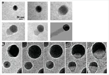
in-situ observation of two growths: one of germanium nanowires in
the chamber of a TEM equipped with a platinum chau ante [78] and
one of nano ls of silicon in an environmental MET (ETEM) [79]. For
the first, pure germanium served as a strong precursor and catalyst
gold. The gas is transported by heating the system to a temperature
between 700 C and 900 C. Figure 11a shows a set of sequential
TEM images recorded during the growth of a Ge nanowire. These
images clearly show the steps of the illustration in (figure 11a): the
formation of the alloy, the nucleation of the Ge nanocrystal from
the drop and the growth of the nanowire where one can see the
dice. Placement of the Au-Ge interface. On the second observation
presented in (Figure 11b), we observe the formation of the alloy
and the nucleation of a silicon nanowire see (Figure 10).
Figure 11: a): Formation of a Ge nanowire by VLS from a gold particle observed in situ [78], b) formation of a Si nanowire by VLS observed in situ also [79].
Based on this mechanism, it is possible to control several aspects of growth. As a first approximation, the diameter of each nanowire is largely determined by the size of the catalyst. Smaller catalysts give smaller threads. It has been demonstrated that Si and GaP nanowires with a specific diameter can be obtained by controlling the diameter of gold colloids in solution used as catalysts [40, 81, 82]. The VLS method is now widely used to create 1D nanostructures for a diverse range of inorganic materials that include elementary semiconductors (Si, Ge and B) [75, 83, 84], III-V semiconductors (GaN, GaAs, GaP , InP, InAs) [76, 85-86], semiconductors II-VI (ZnS, ZnSe, CdS, CdSe) [74, 87-88] and oxides (ZnO, MgO, SiO2) [89,90]. Among these materials, compound semiconductors, such as GaAs, GaN, ZnO and CdSe, are of particular interest because of their band gap which allows optical and optoelectronic applications. The nanowires produced by VLS process are remarkable for their uniformity of diameter. When growth is complete, finding the drop of catalyst at one end of the nanowire is evidence of the VLS mechanism.
A. Production or dispersion of catalytic particles:
The VLS mechanism, as a catalytic mechanism, requires the use of a catalyst. As a first approximation, the shape of the catalyst must be a drop whose diameter corresponds to the diameter of the desired nanowire. It is possible to obtain this type of particles either by dewetting a gold film or by using gold colloids.
B. Dewetting:
Dewaxing a continuous thin film consists of making it undergo a heat treatment that will provide energy to the system allowing it to retract to form a set of drops on the entire surface. The system then tends to its most stable thermodynamic conguration. This configuration is a function of the surface condition of the substrate (roughness, grain boundaries, etc.), the surface energy of the substrate, the interaction energy between the thin layer and the substrate, and others. energy factors. The experimental levers that will make it possible to vary the values of these energies are the thickness of the continuous film, the temperature of the annealing and the duration of the heat treatment. Obtaining catalytic nanoparticles by dewetting has the advantage of being a method compatible with microelectronics because it uses standard vacuum heat treatments.
The objective after the dewetting step is to have the most homogeneous catalyst drops possible on the substrate. The thickness of the deposited thin film reported in the literature varies between 0.5 nm and 20 nm [91-93]. The size of the particles depends essentially on the thickness of the deposited catalyst layer. A relatively long annealing time (20-30 min) allows having homogeneous drops and more scattered on the support. With thicker catalyst layers, it is necessary to reduce this duration so as not to have too large drops. However, this causes a less homogeneous distribution of the drops. It is common practice to etch the surface of the silicon substrate prior to gold deposition. The objective is to remove any organic residues but especially the native oxide present on the surface of the Si substrate. We will see later the influence of this chemical attack on the growth of nanowires.
C. Gold Colloid Dispersion
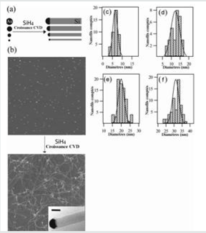
It is also possible to obtain catalytic gold particles from chemically synthesized and commercially available solution gold colloids for diameters ranging from 2 to 30 nm. Gold colloids in solution (or colloidal solution) are aggregates of gold stabilized by a set of organic molecules, which we will later call organic gangue, which stabilizes the aggregates and prevents them from coalescing with each other. Colloids, having diameters of 5, 10, 20 and 30 nm, gave rise to nanowires with average diameters of 6, 12, 20 and 31 nm respectively (Figure 12) and [81]. The density of nanowires obtained on the substrate will be a function of the number of particles present at the origin, there will be no more nanowires. However, there may be fewer particles than particles because the reactivity of all particles is not guaranteed. The advantage of this method of obtaining the catalyst is the calibration of the diameters of the gold particles and the low dispersion around the value of the average diameter. Potentially difficult points are the removal of the organic gangue before the growth and the dispensing of the colloids in a homogeneous and dense way on the substrate before the growth.
Figure 12: (a) Diagram of diameter control by size of gold nanoparticles. (b) AFM image of 10 nm diameter gold colloids and SEM image of the obtained nanowires; nanowire 20.6 nm in diameter in the inserted image. (c-f) Histograms and distribution curves of gold colloids and nanowires, respectively, for colloid diameters of 5, 10, 20 and 30 nm [81].
D. Precursor gases
The growth of silicon nanowires by CVD requires the use of a silicon precursor gas such as silane (SiH4), disilane (Si2H6), tetrachlorosilane (SiCl4), dichlorosilane (DCS or SiH2Cl2) or else a mixture of silane and hydrochloric acid (HCl). A large part of the syntheses of silicon nanowires are made from silane, SiH4. We will discuss here the effect of different gaseous precursors on the growth of nanowires according to the data of the literature.
E. Synthesis from tetrachlorosilane (SiCl4):
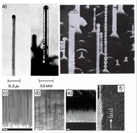
The first silicon nanowires were discovered by the team of Wagner and Ellis in 1964 from a mixture of SiCl4 and H2 [72]. A second synthesis of nanowires from SiCl4 was carried out in 1973. It was at the end of these syntheses that the vapor-liquid-solid mechanism was proposed to explain the growth of nanowires [94]. As the tetrachlorosilane is a liquid precursor, bubbling of the carrier gas is necessary in order to convey the droplets in the gas phase. The tetrachlorosilane being little reactive, the syntheses are carried out at a higher temperature than with silane. These first nanowires were of micrometic size with diameters of more than 500 nm. Subsequently, the thickness of the gold film was decreased to 5 nm resulting in films of 30-40 nm [95,96]. It has also been observed diameter oscillations for these nanowires, specificity that will not be found in the following growths. These oscillations have been attributed to instability which depends in part on the ratio Cl / H and the temperature. Instability occurs with high Cl/H ratios and temperatures above 1020°C [94]. Two other growths have shown that straight nanowires for lower temperatures of 900°C [83] and 1000? C [96], may tend to curl if they are long. To summarize, these growths show a change of morphology (oscillations, curvatures) for nanowires synthesized at 1000°C and more, and for high Cl / H ratios (Cl / H = 1.5.10). The images of these growths are grouped together in Figure 13. One of the 2 growths led to the observation of very fine nanowires 10 nm in diameter [83]. Localized growth has been achieved and has enabled the fabrication of silicon nanowire diodes [97]. Growth with tetrachlorosilane and a nickel catalyst has also been reported [83, 98]. Like dichlorosilane, tetrachlorosilane forms HCl as a reaction by-product. The role of HCl was mentioned only once among growths from tetrachlorosilane, for growth greater than 800°C. In this case, it is said that hydrochloric acid acts as an engraving element. However, the etching is not observed on the nanowires but only on the substrate. This single result does not allow to rule on the influence of HCl. With tetrachlorosilane as a precursor gas, growth temperatures are above 800°C and up to 1250°C. The nanowires obtained are grown on cleaned substrate i.e. without native silica. They are perpendicular to the substrate and have a clean base that would be due to the action of HCl, a by-product of the reaction, during growth. The four growth variants on substrate <111> are found.
Figure 13: Growth from SiCl4: TEM (a) and SEM images (b) of Si whiskers with and without oscillations [72, 94]. SEM images in section (c-e) and MET (f) of Si nanowires [95].
F. Synthesis from disilane(Si2H6)
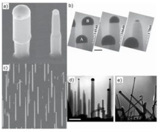
Due to the high reactivity of disilane, growths from disilane are carried out in lower temperature ranges (450-600°C) than those of tetrachlorosilane. A study of the growth of nanowires under an ultrahigh vacuum has been conducted [99-102]. Despite the differences with the more common growths performed at higher pressure, these syntheses have provided answers to gold diffusion capabilities and influence of the oxygen supply during the reaction. (Figure 14)shows nanowires synthesized from Si2H6. Recently, it was realized a low temperature synthesis (350°C) using disilane because its decomposition is possible at low temperature (350- 400°C). Achieving growth at 350°C has the advantage of avoiding the coalescence of gold drops and thus synthesizing fine nanowires (8 ± 5 nm) [102].
Figure 14: Growth under ultraviolet from disilane. (a) Change in size of the drops during growth. (b) Disappearance of a drop during growth. (c) Small growth. Growth (d) without and (e) with addition of oxygen in section [99-101].
G. Synthesis from dichlorosilane (SiH2Cl2)
The growth of silicon nanowires from DCS is mentioned only once in the literature [103]. The catalyst used is not gold but TiSi2 which is also used for the first time as a nanowire catalyst. Despite a growth mechanism different from that of silicon nanowires made from gold and silane (the titanium-silicon eutectic is at 1330°C), the growths made from TiSi2 with DCS and silane can give some comparisons. At 640°C, the behavior is the same from SiH4 and SiH2Cl2. Each of the gases, SiH4 and DCS, has two kinetic regimes, and only differs the transition temperature between these two regimes. For the silane, the transition is close to 800°C and for the DCS; it is around 1000°C. The growths realized at 920°C give very different results from one gas to another. With silane, the growth of nanowires and the growth of the silicon are fast. Long nanowires are obtained as in the image b) of (Figure 15). Whereas with DCS, the growth of nanowires is much slower and, despite non-catalytic deposition, which is also slower than with silane, the nanowires are still surrounded by the catalytic silicon layer (see image (Figure 15).
Figure 15: Silicon nanowires from a) DCS obtained at 920°C and b) SiH4 obtained at 670°C with a TiSi2 catalyst (sectional view) [103].
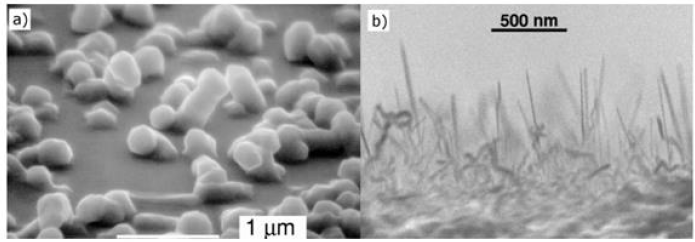
In an attempt to explain the presence of the non-catalytic silicon
layer and the difference in reactivity of the two gases, it is useful to
look at the behavior of the silane and DCS used as precursors for
the growth of a full silicon layer. Non-catalytic silicon deposition
is favored for silane over DCS for two reasons. The first is that
the activation energy to create a silicon layer from silane is 41.5
kcal.mol-1 (174 kJ.mol-1) [104] whereas from DCS it is about 57
kcal.mol-1 (239 kJ.mol-1) [105]. The silane is more reactive than dichlorosilane, so silicon deposition will be faster with the silane
for the same reaction temperature. The second reason is that DCS
brings chlorine, which will have two effects. On the one hand, at high
temperature and high pressure, hydrochloric acid will burn silicon
whether it is full-length or nanowires. On the other hand, under
reduced pressure and for a high Cl/H ratio, the chlorine will both
retain the silicon in the gas phase in the Si-Cl or Si-Cl-H forms and
thus slow or even prevent the deposit of silicon but also to attach
to the surface of the substrate, decreasing the number of possible
nucleation sites for silicon deposition [104]. To return to the
nanowires, with silane, the catalytic growth dominates what gives
nanowires of 2 to 3 microns whereas with the DCS, the catalytic and
non-catalytic growths are equivalent which gives short nanowires
and diameters of several hundreds of nanometers due to the radial
growth of silicon [103].
The selectivity of SiH2Cl2 observed during the growth of thin
layers is not found in growth of nanowires. However, the presence of
HCl as a by-product of the reaction makes it possible to slow down
the development of the high temperature non-catalytic silicon layer
in the case of TiSi2 island-catalysed growth of nanowires. To date,
there has been no report of growth of silicon nanowires by the
vapor-liquid-solid method from SiH2Cl2.
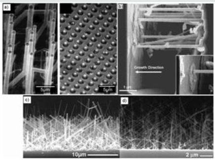
H. Synthesis from a mixture of silane (SiH4) and hydrochloric acid (HCl):
Synthesis from a mixture of silane (SiH4) and hydrochloric acid (HCl) several syntheses using a mixture of silane and hydrochloric acid as gaseous precursors were carried out [106-109], so far as it has not been brought to light an obvious effect of hydrochloric acid. Within a single team, it has been found that by increasing the Cl/Si ratio from 2 to 6, the average diameter decreases from 100 nm to 35 nm [208]. Figure 16 shows the nanowires made with HCl in a template (a), bypass (b) and in full layer (a and c). It should be noted that this mixture SiH4 -HCl is also used for the growth of p-doped nanowires to boron and gives straight lines [108,109]
Figure 16: Growth from a mixture of SiH4 and HCl. (a) Nanowires obtained at 800°C in simple forest and integrated in a hole device [106]. (b) Bridged nanowires seen in section between two trenches oriented <111>[107]. (c) Nanowires made at 670°C from a film of 5 nm gold and (d) at 680°C from 1 nm of gold seen in section [108].
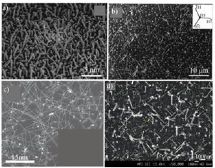
I. Synthesis from silane (SiH4): Sy
nthesis from silane (SiH4) The “silane” trio as a precursor
gas, “gold” as catalyst and “silicon” as substrate is the most used
for the growth of silicon nanowires. It is very widely described in
the literature [81, 75, 110, 111, 96, 212] and serves as a reference
for growth with other precursor gases. (Figure 17)shows some
nanowires synthesized from silane. The temperature of the
eutectic Au / Si is low (363°C) which allows a relatively low growth
temperature and gives finer nanowires by preventing diffusion and
coalescence of the gold particles. According to experimental studies,
Si nanowires made from SiH4 can be up to 10 nm in diameter while
those from SiCl4 are not smaller than 50-100 nm [94]. However,
compared with SiCl4, SiH4 is more expensive and presents more
risks including that of being spontaneously flammable in the air.
It has been shown that by decreasing the silane partial pressure,
the number of morphological defects such as directional changes is
reduced as the diameter of the nanowires increases.
The infuence of the type of gas on the diameter of the
nanowires is mainly a function of the temperature required for
this gas to dissociate and to give nanowires. The higher it is, the
larger the diameter will be. The size of the catalytic particle and,
consequently, the diameter of the nanowire, remain very strongly
related to the thickness of the gold film or the size of the pads.
The influence of HCl is not yet clearly interpreted; some articles
evoke an effect on the base of the nanowire or on the diameter of
nanowires according to the ratio Cl/Si whereas others who use it do
not draw any conclusion.
Figure 17:Growth from SiH4: a) on an Si substrate (100) with a biased thermal oxide layer [111], b) on an Si substrate (111), c) on a Si substrate (100) [112] and d) also on a substrate Si (100) [110] seen in cross-section b, d).
J. Metal catalyzed electroless etching MCEE
In 2002, Peng et al. produced silicon nanowires at the waferscale
via simple, cheap chemical etching methods. Their techniques
consisted of immersing silicon in an HF-AgNO3 solution at room
temperature. They obtained SiNW and nanostructures with a
high degree of orientation. They also produced porous silicon and
silicon nanoholes by MCEE, which involves etching silicon wafers in
an aqueous HF/Fe (NO3)3 or H2O2sub> solution [113].
The underlying mechanism proposed for MCEE was based on a
metal-induced local oxidation and anisotropic dissolution of silicon
in the aqueous oxidizing HF acid solution. They observed that the
metal moved preferentially to the Si (100) orientation, causing
anisotropic etching. They also compared MCEE to chemical vapor
deposition and Reactive Ion Etching and concluded that MCEE is a
simple, low-temperature, scalable, and speedy process.
MCEE has been used to produce vertical SiNWs with diameters
from 20-300 nm, which maintained the orientation of the starting
substrate, and showed desirable electrical properties [114]. Due
to its flexibility in wafer scale production and ability to fabricate
vertically aligned SiNW arrays, MCEE is considered a cheaper
alternative to common top-down etching techniques [115]. MCEE
fabricated nanowires are uniform in terms of their doping profile,
crystal orientation, density, size, and shape, which are essential for
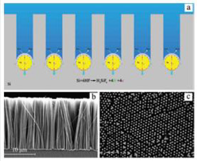
photovoltaic applications. For instance, by combining MCEE and
nanosphere lithography, researchers obtained SiNWs of controlled
diameters, densities, and lengths (Figure 18) [116, 117].
Figure 18: a) Schematics illustration of MCEE process. b) Cross section of silicon nanowires produced by metal catalyzed electroless etching MCEE. c) SEM image of ordered arrays of SiNWs with controlled diameter and density by combination of MCEE and nanosphere lithography techniques [117].
Conclusion
Nanowires are nanostructures, with the diameter of the order of a nanometer (10-9 m). Alternatively, the nanowires can be defined as structures that have a thickness or diameter limited to a few tens of nanometers or less, and a length without constraint. At these scales the quantum effects are important - hence the use of the term "quantum wires". Many types of nanowires exist, including metallic (for example, Ni, Pt, Au), semiconductor (e.g., Si, InP, GaN, etc.), or dielectric (e.g., SiO2, TiO2) materials. Molecular nanowires are made up of repeating organic (eg DNA) or inorganic (Mo6S9-xIx) molecular units. These nanometric objects are of interest for many fields of technology (micro/nanoelectronics, photovoltaic energy) and scientific (biology, physics). In this review we were interested in the wide range of existing nanowires as well as in the synthesis techniques used.
Acknowledgments
The authors are thankful to Center of Research Excellence in Renewable Energy (CoRERE), King Fahd University of, Petroleum and Minerals for the support in this work.
References
- XF Duan,S Zafar, C D’Emic, A Jagtiani, E Kratschmeret al. (2001) Nature ACS Nano 12(7): 6577-6587.
- MSGudiksen, et al.(2002) Nature 415: 617.
- Y Huang, et al.(2001) La Science 294: 1313.
- MT Bj, et al.(2002) Nano Lett 2: 87.
- Iijima(1991)Helical Microtubules of Graphitic Carbon. Nature, 354(6348):56-58.
- Rao and A. Govindaraj(2005) Nanotubes and Nanowires. 113: 375-392.
- R Bosisio, GFleury, C Gorini& JL Pichard(2017)Advances in Physics: X 2(2):344-358
- S Rahong T Yasui, N Kajiabd and Y Baba (2016) Lab Chip 16: 1126-1138.
- G Bonnier and E Devin(1997)Les Techniques de l'Iingénieur R 2(590):1-22.
- X Kleber, V Massardier,J Merlin (2005) Les Techniques de l'Ingénieur RE 39:1-9.
- R Venkatasubramanian, E Siivola, T Colpitts, B O'Quinn(2001) Nature 413:597-602.
- KF Hsu (2004)Science, pages 818-821.
- A Majumdar, A Ali, Y Chen, V Vasiraju and S Vaddirajuet al.(2017) Nanotechnology Science303:777-778.
- CB Vining (2001) Semiconductors Are Cool. Nature, 413:577-578.
- YS Touloukian, RW Powell, CY Ho, and PG Klemens(1970) Thermophysical Properties of Matter 1(339).
- S Mukherjee, U Givan, S Senz, M de la Mata,O Moutanabbir(2018) Nano Letters 18(5): 3066-3075.
- AI Boukai, Y Bunimovich, J Tahir Kheli, JK Yu, and JRHeath,et.al(2008) Nature 451:168-171.
- GS Nolas, J Sharp, HJ Goldsmid (2001) Thermoelectrics.
- YS Ju, KE Goodson(1999) Applied Physics Letters 74:3005-3007.
- D Li, Y Wu, P Kim, L Shi, A Majumdar, et.al(2003) Applied Physics Letters 83(14): 2934-2936.
- TC Harmann, PJ Taylor, MP Walsh, and BE Laforge(2002) Science 297: 2229-2232.
- DY Li, Y Wu, R Fan, PD Yang, A Majumdar (2003) Applied Physics Letters S 83(15): 3186-3188.
- NA Melosh, A Boukai, F Diana, B Gerardot, A Badolato(2003) Science 300(5616): 112-115.
- Tian, X Zheng, TJ Kempa, Y Fang, and N Yu et.al (2007) Nature 449:885-889.
- Zhang, Y Liu, H Crystals(2019) 9: 87B.
- L Tsakalakos, J Balch, J Fronheiser, BA Korevaar, O Sulima, et.al (2007) Applied Physics Letters 91(233117): 1-3.
- G Andrä, M Pietsch, T Stelzner, F Falk, E Ose, et.al.(2007) Nanowires for Thin Film Solar Cells. 22nd Europ. Photovoltaic Solar Energy Conference and Exhibition.
- K Bullis(2007) Tiny Solar Cells: Photovoltaics Made of Nanowires Could Lead to Cheaper Solar Panels MIT Technology Review.
- M BechelanyNouveau Procédé de Croissance de Nanofillsà Base de SiC et de Nanotubes de BN, étude des Propriétés Physiques d'un NanofillIndividuelà Base de SiC.Thèse de Doctorat, Université Claude Bernard - LYON I, 2006.
- B Gates, B Mayers, B Cattle, and YN Xia, (2002) Advanced Functional Materials 12(3): 219-227.
- B Mayers and YN Xia(2002) Journal of Materials Chemistry 12(6): 1875-1881.
- B Messer, JH Song, M Huang, YY Wu, F Kim, et.al (2000) Advanced Materials 12(20):1526-1528.
- JH Song, B Messer, YYWu, H Kind,PD Yang, et.al (2001) Journal of the American Chemical Society 123(39): 9714-9715.
- TJ Trentler, KM Hickman, SC Goel, AM Viano, and PC Gibbons, et.al (1995) Science 270(5243): 1791-1794.
- SD Dingman, NP Rath, PD Markowitz, PC Gibbons, WE Buhro(2000)Angwandte Chemie-International Edition 39(8): 1470-1472.
- TJ Trentler, SC Goel, KM Hickman, AM Viano,MY Chiang(1997) Journal of the American Chemical Society 119(9): 2172-2181.
- PD Markowitz, MP Zach, PC Gibbons, RM Penner, WE Buhro(2001) Journal of the American Chemical Society 123(19): 4502-4511.
- JD Holmes, KP Johnston, RC Doty, BA Korgel(2000) Science 287(5457): 1471-1473.
- XM Lu, T Hanrath, KP Johnston, BA Korgel(2003) Nano Letters 3(1): 93-99.
- BGelloz, YCoffinier, BSalhi, NKoshida, GPatriarche, et.al. (2006) MRS Proceedings.
- YN Xia, PD. Yang, YG. Sun, YY. Wu, B. Mayers, et.al. Advanced Materials, 15(5): 353-389.
- X Wang and Y Li (2002) Journal of the American Chemical Society 124(12): 2880-2881.
- JR Heath and FK Legoues(1993) 208(3-4): 263-268.
- T Kasuga, M. Hiramatsu, A Hoson, T Sekino, K Niihara (1998) Formation of Titanium Oxide Nanotube. Langmuir 14(12): 3160-3163.
- QH Zhang, LA Gao, J Sun, S Zheng(2002) Chemistry Letters (2): 226-227.
- Y Xie, P Yan, J Lu, WZ Wang, YT Qian(1999) Chemistry of Materials 11(9): 2619-2622.
- YD Li, M Sui, Y Ding, GH Zhang, J Zhuang, et.al (2000) Advanced Materials 12(11): 818-821.
- H Ringsdorf, B Schlarb, and J. Venzmer(1988)Angewandte Chemie-International Edition in English 27(1): 113-158.
- A Govindaraj, FL Deepak, NA Gunari, CNR Rao(2001) Israel Journal of Chemistry 41(1): 23-30.
- CNR Rao, A Govindaraj, FL Deepak, NA Gunari, M Nath(2001)Applied Physics Letters 78(13): 1853-1855.
- MJ Zheng, LD Zhang, XY Zhang, J Zhang, GH Li(2001) Chemical Physics Letters 334(4-6): 298-302.
- CR Martin, Science (1994). 266(5193): 1961-1966.
- D Almawlawi, CZ Liu, M Moskovits(1994) Journal of Materials Research 9(4): 1014-1018.
- JCHulteen and CR Martin (1997) Journal of Materials Chemistry 7(7): 1075-1087.
- RL Fleisher, PB Price, RM Walker (1975) University of California Press Berkeley CA.
- A Despic, VP Parkhulik(1989) Modem Aspects of Electrochemistry, volume 20. Plenum Press, New York.
- KK Lew and JM Redwing(2003) J. Journal of Crystal Growth 254(1-2): 14-22.
- Huczko(2000) Applied Physics A-Materials Science and Processing, 70(4): 365-376.
- KB Shelimov, M Moskovits(2000) Chemistry of Materials 12(1): 250-254.
- G Schmid(2002) Journal of Materials Chemistry 12(5): 231-1238.
- N Li, XT Li, WC Geng, L Zhao, GS Zhu, et.al (2005) Materials Letters 59(8-9): 925-928.
- ST Lee, NWang, YF Zhang, YH Tang, Mrs Bulletin (1999) 24(8): 36-42.
- N Wang, YH Tang, YF Zhang, CS Lee, ST Lee(1998) Physical Review B 58(24): 16024-16026.
- N Wang, YH Tang, YF Zhang, CS Lee, I Bello(1999) Chemical Physics Letters 299(2): 237-242.
- JL Gole, JD Stout, WL Rauch, ZLWang (2000) Applied Physics Letters 76(17): 2346-2348.
- DDD Ma, CS Lee, FCK Au, SY Tong,ST Lee, Science(2003) 299(5614): 1874-1877.
- SH Wang and SH Yang (2001) Chemistry of Materials 13(12): 4794-4799.
- X Jiang, T Herricks,Y Xia (2002)CuO,Nano Letters 2(12):1333-1338.
- Y Yin, G Zhang, Y Xia (2002) Advanced Functional Materials 12(4): 293-298.
- YJ Xiong, BTMayers, YN Xia (2005) Chemical Communications 40: 5013-5022.
- YJ Zhang, NL Wang, SP Gao, RR He, S Miao (2002) Chemistry of Materials 14(8): 3564-3568.
- GC Yi, CR Wang,WI Park (2005) Semiconductor Science and Technology 20(4): S22-S34.
- RS Wagner and WC Ellis(1964) Applied Physics Letters 4(5): 89-90.
- BSalhi, B Grandidier R Boukherroub(2006) Journal of Electroceramics Volume (16), N° 1: 15-21.
- X Duan CM Lieber (2000) Advanced Materials12(4): 298-302.
- J Westwater, DP Gosain, STomiya, S Usui(1997) Journal Vacuum Science Technology B 15(3): 554-557.
- M Yazawa, M Koguchi, A Muto, K Hiruma(1993) Advanced Materials 5(7-8): 577-580.
- H Abed, A Charrier, H Dallaporta, V Safrarov, H Jangotchian, et.al.(2006) Journal of Vacuum Science and Technology B 24(3): 1248-1253.
- YY Wu PD Yang (2001) Journal of the American Chemical Society 123(13): 3165-3166.
- S Hofmann, R Sharma, CT Wirth, F Cervantes Sodi, C Ducati (2008) Nature Materials Letters 7: 372-375.
- MS Gudiksen CM Lieber (2000) Journal of the American Chemical Society 122(36): 8801-8802.
- Y Cui, LJ Lauhon, MS Gudiksen, J Wang, CM Lieber (2001) Applied Physics Letters 78(15): 2214-2216.
- YY Wu, HQ Yan, M Huang, B Messer, JH Song, et.al (2002) Chemistry- A European Journal 8(6): 1261-1268.
- Y Zhang, Q Zhang, N Wang, Y Yan, H Zhou, et.al (2001) Journal of Crystal Growth 226:185-191.
- YY Wu and PD Yang (2000) Chemistry of Materials 12(3): 605.
- CC Chen, CC Yeh, CH Chen, MY Yu, HL Liu (2001) Journal of the American Chemical Society 123(12): 2791-2798.
- K Hiruma, M Yazawa, T Katsuyama, K Ogawa, K Haraguchi(1995) Journal of Applied Physics 77(2): 447-462.
- YWWang, LD Zhang, CH Liang, G Z.Wang,XS Peng (2002) Chemical Physics Letters 357(3-4): 314-318.
- M Lopez Lopez, A Guillen Cervantes, Z Rivera Alvarez,I Hernandez Calderon (1998) Journal of Crystal Growth 193(4): 528-534.
- YJ Chen, JB Li, YS Han, XZ Yang, JH Dai(2002) Journal of Crystal Growth 245(1-2): 163-170.
- XC Wu, WH Song, KY Wang, T Hu, B Zhao, et.al(2001) Chemical Physics Letters 336(1-2): 53-56.
- V Schmidt, SSenz,U GöseleZ Metallkd(2005) UHV Chemical Vapour Deposition of Silicon 96(5): 427-428.
- A Dupuis (2005) Progress in Materials Science 50(8): 929-961.
- Y Wakayama S Tanaka (1999) Surface Science 420: 190-19.
- EI Givargizov(1973) Journal of Crystal Growth 20: 217-226.
- AI Hochbaum, R Fan, R He P Yang (2005) Nano Letters 5(3): 457-460.
- AMao, HT NgP Nguyen, M McNeil,M Meyyappan(2005) Journal of Nanoscience and Nanotechnology 5: 831-835.
- JB Jackson, D Kapoor, SG Jun, MS Miller (2007) Journal Applied Physics 102(054310): 1- 6.
- N Wang, Y Zhang, J Zhu (2001) Journal of Materials Science Letters 20: 89- 91.
- JB Hannon, S Kodambaka, FM Ross,RM Tromp (2006) Nature 440(04574): 69-71.
- S Kodambaka, J Terso, MC Reuters,FM Ross (2006) Physical Review Letters 96(096105): 1- 3.
- S Kodambaka, JB Hannon, RM Tromp,FM Ross (2006) Nano Letters 6(6): 1292-1296.
- S Akhtar, K Usami, Y Tsuchiya, H Mizuta,S Oda(2008) Applied Physics Express 1(014003): 1-3.
- TI Kamins, R StanleyWilliams, DP Basile, T Hesjedal, JS Harris(2001) Journal of Applied Physics, 89(2): 1008-1016.
- S Bodnar, Thèse de Doctorat, Institut National des Sciences Appliquées de Toulouse.
- G Savelli Thèse de Doctorat(2007) Université Joseph Fourier de Grenoble.
- L Ganglo, E Minoux, KBK Teo, P Vincent, VT Semet, et.al. (2004) Nano Letters 4(9): 1575-1579.
- S Sharma, TI Kamins, RS Williams(2005) Applied Physics A 80: 1225-1229.
- S Sharma, TI Kamins, MS Islam, RS Williams,AF Marshall(2005) Journal of Crystal Growth 280: 562-568.
- TI Kamins, S Sharma, AA Yasseri, ZLi, J Straznicky(2006) Nanotechnology, 17: S291-S297.
- V Schmidt, S Senz, U. Gösele(2005) Nano Letters, 5(5): 931-935.
- XW Zhao FY Yang (2008) The Journal of Vacuum Science and Technology B 26(2): 675-677.
- SJ Whang, S Lee, DZ Chi, WF Yang, BJ Cho, et.al.(2007) Nanotechnology 18(275302): 1-4.
- KQ Peng, YJ Yan, SP GAO, J Zhu, Adv Mater(2002) 14: 1164, KQ. Peng, YJ. Yan SP. GAO, J Zhu, Adv Mater(2002) 14, 1164, a) KQPeng, AJ Lu, RQ Zhang, ST Lee, Adv Funct Mater(2008) 18: 3026, b) KQ Peng, X Wang, XL Wu, ST Lee (2009) Appl. Phys Lett, 95, 143119, c) KQ Peng, X Wang, ST Lee(2009) Appl Phys Lett, 95: 143119.
- Colin D Bailie, M Greyson Christoforo, Jonathan P Mailoa, Andrea R Bowring,a Eva L Unger (2015) Energy Environ Sci 8: 956–963.
- B Salhi, MK Hossain, F Al-Sulaiman(2018) 161: 180-186.
- KQ Peng, AJ Lu, RQ Zhang, ST Lee, Adv Funct. Mater(2008) 18: 3026,b) KQ Peng, X Wang, XL Wu, ST Lee,(2009) Appl Phys Lett, 95: 143119, c) KQ Peng, X Wang, ST Lee, (2009) Appl Phys Lett, 95: 143119, KQ Peng, ML Zhang, AJ Lu, NB Wong, RQ Zhang, et.al.(2007)ApplPhys Lett, 90: 163- 123.
- ZP Huang, H Fang, J Zhu (2007) Adv. Mater, 19: 744, b) H Fang, Y W, JH Zhao, J Zhu, (2006) Nanotechnology 17: 3768.

Top Editors
-

Mark E Smith
Bio chemistry
University of Texas Medical Branch, USA -

Lawrence A Presley
Department of Criminal Justice
Liberty University, USA -

Thomas W Miller
Department of Psychiatry
University of Kentucky, USA -

Gjumrakch Aliev
Department of Medicine
Gally International Biomedical Research & Consulting LLC, USA -

Christopher Bryant
Department of Urbanisation and Agricultural
Montreal university, USA -

Robert William Frare
Oral & Maxillofacial Pathology
New York University, USA -

Rudolph Modesto Navari
Gastroenterology and Hepatology
University of Alabama, UK -

Andrew Hague
Department of Medicine
Universities of Bradford, UK -

George Gregory Buttigieg
Maltese College of Obstetrics and Gynaecology, Europe -

Chen-Hsiung Yeh
Oncology
Circulogene Theranostics, England -
.png)
Emilio Bucio-Carrillo
Radiation Chemistry
National University of Mexico, USA -
.jpg)
Casey J Grenier
Analytical Chemistry
Wentworth Institute of Technology, USA -
Hany Atalah
Minimally Invasive Surgery
Mercer University school of Medicine, USA -

Abu-Hussein Muhamad
Pediatric Dentistry
University of Athens , Greece

The annual scholar awards from Lupine Publishers honor a selected number Read More...


