Lupine Publishers Group
Lupine Publishers
Menu
Research ArticleOpen Access 
Nanotechnology in Wireless Communication Volume 1 - Issue 4
D S Grewal*
- Bhai Maha Singh College of Engineering. Muktsar, Director Principal, India
Received: January 7,2022 Published: February 2,2022
Corresponding author: D S Grewal, Bhai Maha Singh College of Engineering. Muktsar, Director Principal, India
DOI: 10.32474/JBRS.2022.01.000119
Abstract
Nanotechnology is the projected ability to construct items at nanoscale from the bottom up, using techniques and tools being developed today to make complete, high-performance products. Nanotechnology for wireless communication will add on high quality, low cost, high sensitivity, reliability, robustness, high accuracy and computer function- ability. Though it has initial high research, development and manufacturing costs yet that can be compensated by low bulk manufacturing costs. Portable energy storage using super capacitor-battery hybrids based on new materials including carbon nano-horns and porous electrodes, fuel cell technologies, energy harvesting, and more efficient solar cells will help increase life of energy sources and transportability and reduce size and equipment weight Electronics and computing advances reaching beyond IC scaling limits, new computing approaches and architectures, embedded intelligence and future memory technologies, nano-scale transducers for mechanical, optical and chemical sensing, bio-mimetics in sensor signal processing and nano-scale actuation will increase network intelligence and efficiency.
The concept of ambient intelligence could result in our living environment in the home, car and office becoming sensitive and responsive to our presence. For continuous and much simpler interaction with information to enhance quality of life, improve working conditions and increase productivity appliances such as computers, multimedia equipment and communications devices would be integrated into that environment. Flexible mobile phones able to act at the same time as personal digital assistants (PDA), electronic purses and interactive media providers will be available at an affordable cost. Combined mobile communications and global location units will enable the dispatch of assistance quickly to elderly or handicapped people in trouble.
Such recent advances in nano-scale technologies can be exploited not only to lead to new mass markets for electronic communication but also to provide the high-technology experience and low-cost manufacturing expertise required to develop other nanotechnology industries
Keywords: Nanotechnology; Nanomaterials; Wireless Communication; Ambient Intelligence
Introduction
These days we describe the advancements in wireless technologies in the form of generations. Presently we are going through the second generation (2G) and are about to enter third generation (3G) and have started planning for fourth generation (4G) and dreaming of fifth generation (5G). Nanotechnology is going to be the key technology to help this great change. The purpose of this paper is to outline what we are going to enter soon and then develop on this the 4G and 5G and how this nanotechnology is going to change things, so that we may know as to what is in store for us when we are too old to enjoy the benefits while the new generations live the different form of technical life. Our first- and second-generation mobile telephony was intended for voice transmission. The third generation of mobile telephony will serve both voice and data applications. What will be in store of 4G is not yet fully clear, though it is going to be something different, something more advanced in nature from 3G, e.g., an entirely packet switched network with all digital network elements and extremely high available bandwidth. True multimedia capabilities such as high-speed data access and video conferencing to the handset will be provided by 5G system. 4g also holds the promise of worldwide roaming using a single handheld device followed by communication without even moving your lips, transmission of thoughts directly from one mind to another. This may take us to 5G. One of the latest development in the communication is the “nanotechnology”. (nano=10-9) which will help attain this. It is a great wonder that such a seemingly simple communication and information transportation system is going to use “nanotechnology” at a large scale.
Purpose
Purpose of this paper is to discuss the impact of Nanotechnology on wireless communication.
Technology Development in Wireless Communications
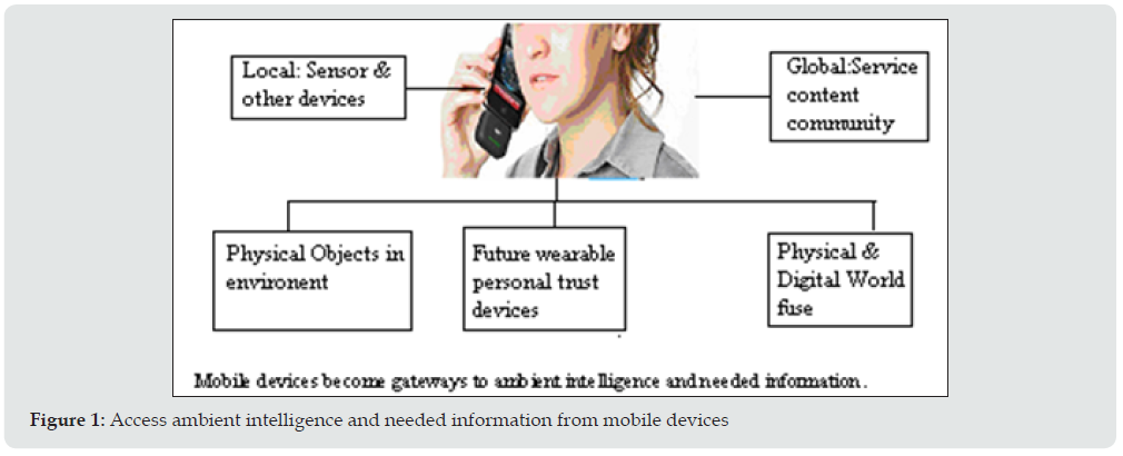
Wireless communication: The term “wireless” [1] has become a generic and all-encompassing word used to describe communications in which electromagnetic waves or RF carries a signal over part or the entire communication path. Wireless industry aims at ambient intelligence. For this the computation and communication should be always available and ready to serve the user in an intelligent way This requires mobile devices embedded in human environment. A new platform with autonomous and robust devices has to be created to enables ubiquitous sensing, computing, and communication (Figure 1). They can be deployed easily, and they survive without explicit management or care. Mobility also implies limited size and restrictions on the power consumption. Seamless connectivity with other devices and fixed networks is a crucial enabler for this. The demands data rates of the wireless links. Intelligence, sensing, context awareness is increased for which more memory and computing power is needed. Severe challenges in thermal management however arise with size limitations.
Future Wireless List of emerging technologies
Short-range point-to-point communication: Wireless microphones, Remote controls, IRDA, RFID (Radio Frequency Identification), Wireless USB, DS RC (Dedicated Short Range Communications), EnOcean, Near Field Communication
Wireless sensor networks: ZigBee, EnOcean; Personal area networks, Bluetooth,
Transfer Jet, Ultra-wideband (UWB from WiMedia Alliance).
Wireless computer networks: Wireless Local Area Networks (WLAN), (IEEE 802.11 branded as WI F i and HiperLAN), Wireless Metropolitan Area Networks (WMAN) and Broadband Fixed Access (BWA) (LMDS,Wi MAX,AIDAAS and HiperMAN. Current technologies cannot resolve these requirements. Nanotechnology has come as a boon to answer most of the requirements of future communications.
Nanotechnology
Nanotechnology is manipulating matter at atomic scale i.e., -1 to 100 nm Each nanometer is only 3 to 5 atoms wide: about 40,000 to 80,000 times smaller than the width of an average human hair. For comparison sizes of other objects are given as under:
a) Fullerenes (C60/Buckyballs) are 1 nm
b) Nanoparticles range from 1 to 100 nm
c) DNA (width) is 2 nm.
d) Proteins range from 5 to 50 nm.
e) Quantum Dots (of CdSe are 8nm))
f) Dendrimers are ~10 nm.
g) Virus range from 75-100 nm.
h) Bacteria range from 1,000 to 10,000 nm.
i) Red Blood cells are ~7000nm in diameter and ~2000 nm in height.
j) White Blood cells are ~10,000 nm in diameter
Like generations of mobile communications, four generations of nanotechnology development are as described in the chart below: (Figure 2) The beginning was from passive nanostructures, materials designed to perform one task. The second phase introduced active nanostructures for multi-tasking; for example, actuators, drug delivery devices, and sensors. The third generation emerging now is expected to feature nano-systems with thousands of interacting components. A few years after that, the first integrated nano-systems, functioning much like a mammalian cell with hierarchical systems within systems, are expected to be developed [2]. Nanotechnology is the projected ability to construct items from the bottom up, using techniques and tools being developed today to make complete, high-performance products. Eric Drexler believed that assemblers could first replicate themselves, building other assemblers. Each generation would build another, resulting in exponential growth until there are enough assemblers to produce objects [3]. Nano-sized materials now emerged as one of the focal points of modem research. The Research & Development in nanotechnology has shown encouraging results giving it global priority. Viable impact of nanotechnology is expected to be visible in next few years.
Applications of Nanotechnology
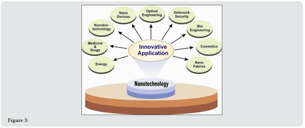
With its promise to revolutionize science, technology and other fields, nanotechnology continues to profoundly impact associated materials, components and systems particularly those used in telecommunications. These developments are leading to easier convergence of related technologies, massive, stored data, compact storage devices and higher performance computing. Nanotechnology will eventually lead to a technology cluster that offers a complete range of functionalities for systems used in domains including information, energy, and construction, environmental and biomedical. Nanostructured opto-electronics materials, MEMS, NEMS, Quantum Dot cellular Automata and Quantum Switching; all these will have vast applications in telecommunication systems [4] (Figure 3).
Applications of Nanotechnology range from -reducing the size of electronic gadgets (Bell Labs has already come out with a selfassembled Transistors of single molecule size) to designing virus to kill bacteria. NNI has expected miniaturized drug delivery system & diagnostic techniques, positive environmental impacts through drastic reductions in energy use, extending & repairing deficits in human senses and security systems smaller than dust. Von Newman has opined Free Energy, while Sarnoff expects Atomic Powered Automobiles soon. The value in Nanotechnology manufacturing is that exact precision is achieved, atom-by-atom. For computers this translates to the next phase of miniaturization as impurities in materials can be eliminated and exacting structures can be assembled. Extremely small and powerful computers will be cheap and abundant, available to even the poorest people. Robotics and artificial intelligence (AI) would provide superhuman capabilities. Ultra-small, highly parallel, computers with multi-teraflop speed Image information processors, e.g., extraction and recognition. Low-power personal and autonomous communication and computation devices high-density information storage devices, e.g., terabit/cm2 nonvolatile memory; lasers and detectors for weapons and countermeasures Optical (infrared, visible, ultraviolet) sensors for improved surveillance and targeting; integrated sensor suites for chemical and biological agent detection; catalysts for enhancing and controlling energetic reactions; synthesis of new compounds (e.g., narrow-band-gap materials). We know today that a quantum computer will outperform any classical computer.
Next, we have “spintronics”, concerned with electromagnetic effects in nanostructures and molecules caused by the quantized angular momentum (the spin) that is associated with all fundamental particles like the electron. The spin dictates the magnetism. Information may be stored and transported in the form of quantized units of magnetism in the future by Manipulating charge and spin on a single electron level. Traditional electronics are changes fast towards new developments due to advances in nano-science and nanotechnology. Sensors, solar cells, electronic paper, bendable touch screens, nanorobots for cancer and COVID 19 are going to change the priorities of science and medicines. Optical signals squeezing through minuscule wires, producing so-called Plasmon; plasmonic circuits moving lots of data and improving the resolution of microscopes, the efficiency of light-emitting diodes, and the sensitivity of detectors are the new directions of change. Making things invisible is also not very far to seek. Grewal explained how the portable nanomaterials will reduce the size of building.
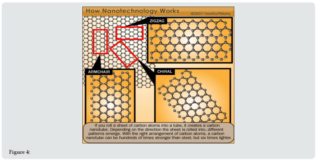
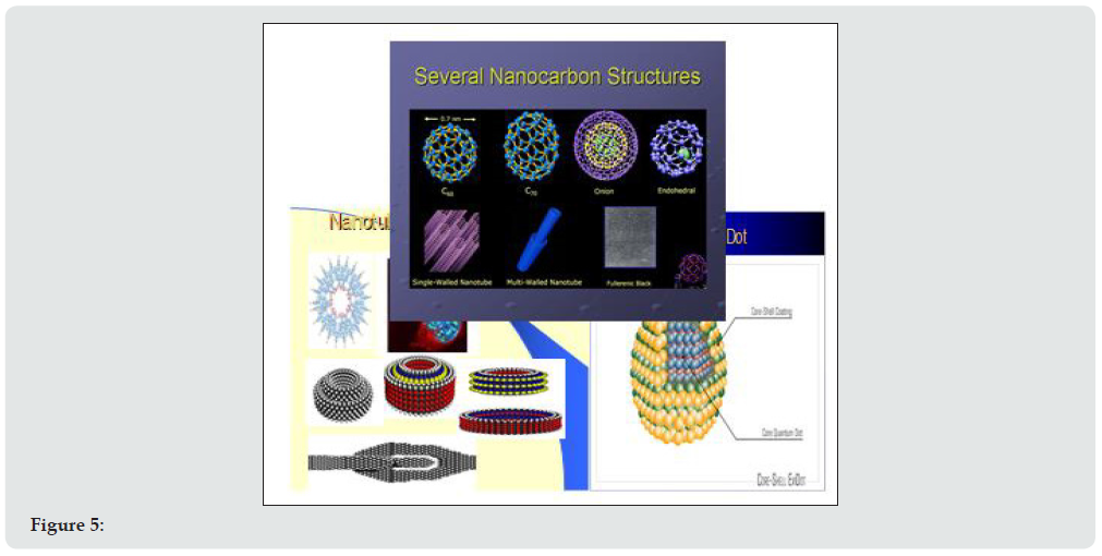
Computers with infinitely great power that compute logarithms to mimic human brains; biosensors that warn us at the early stage of disease and preferably at the molecular level and target specific drugs that automatically attack the disease cells on site; nano-robots that can repair internal damage and remove chemical toxins in human bodies and nano-scaled electronics that constantly monitor our local environment; all these appear to be a few years away kind courtesy nanotechnology (Figure 4). Carbon tubes are one such material which is leading this change speedily. Carbon nanotubes are also making impact in various other fields like molecular nanoelectronics, spintronics, quantum computing, memory & storage, hard drive and tapes, magnetic RAM, optical switching, display technologies etc. currents, they seem to be a wonder material. Many of the extraordinary properties attributed to nanotubes— among them, superlative resilience, tensile strength and thermal stability—have fed fantastic predictions of microscopic robots, dent-resistant car bodies and earthquake- resistant buildings. Different types of spiral structure of nanotubes in a variety of flavors have specific production costs and applications. The Moore’s law has held true for about 40 years now, but the current lithographic technology has physical limits when it comes to making things smaller, and the semiconductor industry, which often refers to the collection of these as the “red brick wall”, thinks that the wall will be hit in around 15 years. The solution would be nanotechnology taking us in the realms of the nano-world from the micro world. With the aid of modern engineering techniques, it is possible to fabricate nano-electronic devices by precise control of the nano-phase materials. The advances in the characterization of nanotube-based AFM tips and the strategies for improved resolution, made DNA based switches and motors real and possible. Conductivity measurements were performed on bundles of single-walled carbon nanotubes with the aid of a scanning tunneling microscope (STM) regarding nano-scale electronic devices. Nanofabrication and nano-electronic devices using carbon nanotube will yield a futuristic approach in electronics engineering. Various nanocarbon structures are as shown in diagram:(Figure 5) Nanotechnology is sometimes referred to as a general-purpose technology. The scale of these physical systems that use nano-scale electronic device is still large and that presents serious challenges to the establishment of interconnections between nano scale devices and the outside world.
Research
Nano technology is now concentrating its research to achieve dramatic, innovative enhancements in the properties and performance of structures, materials, and devices that have controllable features on the nanometer scale (i.e., tens of angstroms). new approaches and processes for manufacturing novel, more reliable, lower cost, higher performance and more flexible electronic, magnetic, optical, and mechanical devices. Various other visionaries have expected it to be better than computer revolution by providing better quality & proved improved means of production. They expect a computer that can make copies of data files at little cost; manufacturing of products to be as cheap as copying of files through nano-factories. These nano-factories will be just like small photocopying machines nano-factory having miniature chemical processors; computing and robotics, producing a wide range of items quickly; cleanly and inexpensively, building products directly from blueprints and with an ability to reproduce own means of production makes it as exponential technology. Nano-materials will be lighter, stronger, smarter and less expensive. New, inexpensive materials are expected with a strength-toweight ratio over 50 times that of steel which shall be Critical for aerospace: airplanes, rockets, satellites, Useful in cars, trucks, ships etc. In computers we expect more than 1021 bits in the same volume, more computing power in the volume of a sugar cube than the sum total of all the computer power that exists in the world today, almost a billion Pentiums in parallel. Storage, conversion, manufacturing improvements by reducing materials and process rates, energy saving (by better thermal insulation for example) and enhanced renewable energy sources are the most advanced nanotechnology projects related to energy.
Potential nanoelectronics and computer technology breakthroughs expected are:
a) Nanostructured microprocessor devices that continue the trend in declining energy use and cost per gate, thereby potentially improving the efficiency of computers by a factor of millions.
b) Higher transmission frequencies and more efficient utilisation of the optical spectrum to provide at least ten times more bandwidth, with consequences in business, education, entertainment and defence.
c) Small mass storage devices with capacities at multi-terabit levels, millions times better than today.
d) Integrated nanosensor systems capable of collecting, processing and communicating massive amounts of data with minimal size, weight and power consumption.
Criteria for Future Development
The key criterion for development however remains i.e., the reduction in size, increase in multiplicity in usage of the same equipment, cost reduction and low energy consumption. Various aspects in the field of nanoelectronics which emerge out of these developments are:
a) Continuous Miniaturisation
b) Continuous Reduction in Cost
c) Lowest Maintenance Costs
d) Least energy use
e) Increased Efficiency with quality products
f) Self-Assembly
g) Replication
h) Multi-usage
i) R & D -Industry-Education-Employment linkage
j) Global Dispersion of R & D and production
k) Political, Economic and Legal Environment
Benefits of Nanotechnology
Nanotechnology is a breakthrough science that combines principles of chemistry, biology and physics to propose microscopic devices on the nano-scale that would mechano-chemically manipulate individual atoms and molecules for the purpose of constructing materials, eradicating disease, and restoring the environment; thus, making the potential benefits of Nanotechnology wide-ranging and revolutionary. Nanotechnology is based on the knowledge that basic biochemical and biophysical processes at work at the molecular level mimic industrial assembly machinery on a microscopic scale. This is perhaps most easily seen in the example of DNA, which is a molecular chain of instructions for building a macroscopic structure from the bottom up. The “tools” that do the actual building are natural biochemical processes. By harnessing those processes in the form of direct manipulation at the atomic level and augmenting them with computerized biomechanical control, a new era of possibility opens.
Reduction of energy consumption
Better insulation systems, the use of more efficient lighting or combustion systems, and use of lighter and stronger materials in the transportation sector can reduce energy consumption. Conversion of electrical energy to light is only about 5% by the current bulbs. LEDs (light emitting diodes) and QCAs (quantum caged atoms) can cause a strong reduction of energy consumption for illumination by nanotechnology.
Increasing the efficiency of energy production
Today’s best solar cells only manage to use 40 percent of the Sun’s energy because of layers of several different semiconductors stacked together to absorb light at different energies and in solar celss purchased from open market give only 15-20% energy, By using nanostructures with a continuum of band gaps the efficiency of light conversion can be increased through nanotechnology. The degree of efficiency of the internal combustion engine is about 30- 40% at the moment. By designing specific catalysts with maximized surface area nanotechnology could improve combustion. A sprayon nanoparticle substance when applied to a surface, instantly transforms it into a solar collector. This was developedbythe University of Toranto in 2005 [5].
Energy Systems
Use of fuel cells powered by hydrogen, ideally produced by renewable energies are examples of an environmentally friendly form of energy. Probably the most prominent nano-structured material in fuel cells is the catalyst consisting of carbon supported noble metal particles with diameters of 1-5 nm. Suitable materials for hydrogen storage contain a large number of small nano-sized pores. Therefore many nano-structured materials like nano-tubes, zeolites or alanates are under investigation. Combustion engine pollutants can be reduced by nano-porous filters. Exhaust can be cleaned mechanically by catalytic converters based on nano-scale noble metal particles. Catalytic coatings on cylinder walls and catalytic nano-particles as additive for fuels can also be cleaned.
Nanobatteries
The use of batteries with higher energy content or the use of rechargeable batteries or super capacitors with higher rate of recharging using nano-materials could be helpful for the battery disposal problem. This will save from large number of discharged batteries.
Information and communication
The critical length scale of integrated circuits is already at the nanoscale (50 nm and below) regarding the gate length of transistors in CPUs or DRAM devices.
Memory Storage
Crossbar switch based electronics have offered an alternative using reconfigurable interconnections between vertical and horizontal wiring arrays to create ultra-high density memories. Two leaders in this area are Nantero which has developed a carbon nano-tube based crossbar memory called Nano RAM and Hewlett- Packard which has proposed the use of memorizer material as a future replacement of Flash memory.
Novel semiconductor devices
Spintronics has brought in a great change. Magneto-resistance effect can be significantly amplified (GMR - Giant Magneto- Resistance) for nanosized objects by the spin of the electrons causing external field. When a is several nanometers thick (e.g., Co- Cu-Co) nonmagnetic layer, separates two ferromagnetic layers the GMR effect leads to a strong increase in the data storage density of hard disks. This is now the gigabyte range is made possible. TMR (tunneling magneto resistance) is very similar to GMR. Both can be used to create a nonvolatile memory known as MRAM (Magnetic Random Acess Memory)
Optoelectronics
In the modern communication technology traditional analog electrical devices are increasingly replaced by optical or optoelectronics devices due to their enormous bandwidth and capacity, respectively. Photonic crystals and quantum dots are going to go a long way to improve optoelectronics
Displays
Using carbon nano-tubes (CNT) displays with low energy consumption can be produced. CNTs (carbon nanotubes as field emitters with extremely high efficiency for field emission display (FED) have been possible due to their small diameter of several nanometers. It operates like CRT (Cathode Ray Tube) though of a small scale,
Quantum Computer
The laws of quantum mechanics for novel quantum computers enabling the fast quantum algorithms are exploited for computing. Qubits (Quantum bit memory space) in quantum computer can carry out several computations at the same time improving performance of old systems.
Nanotechnology Characteristics helping wireless communication are as under:
a) Low cost/high sensitivity
b) High research, development, and initial manufacturing costs; low bulk manufacturing costs.
c) Reliability, robustness, and quality
d) Accuracy
e) Device and system characteristics help biological self-assembly
f) Computer function ability
Possible synergy with ICT
a. Provision of prefabrication and characterization facility.
b. Development of low power, high performance components particularly those associated with optical communication.
c. Integration of technologies for reliable manufacturing.
First transistor using nanotechnology has been found to be 50 times more energy efficient than current models. It can pave the way for communicating the frequencies that are too high for today’s technology. It is made of indium arsenide and the material is selforganized according to a bottom up principle instead of being carved out [6]. The world took a big step closer today to a green and more sustainable communications future with the launch of Green Touch™, a global consortium organized by Bell Labs whose goal is to create the technologies needed to make communications networks 1000 times more energy efficient than they are today [7]. To a great extent Nano-elecetronics was triggered by research on carbon nano-tubes. Before the carbon nano-tubes entered the scene, molecular electronics was the science of organic polymers, their synthesis, processing and doping. With carbon nano-tubes, we finally have a model system at hand that is equally of interest for chemists, material scientists and physicists. While carbon nano-tubes are supra-molecular objects for a chemist, they are one-dimensional solids for a physicist. In the future, more of these supra-molecular structures will be studied on a single molecule level. Companies like, for example Motorola, IBM and Hewlett Packard, are starting to take an active part in this development. Single supra-molecular structures are envisaged as switches and storage media. As has been shown already with DNA molecules, the trend towards molecule will include biological macromolecules as well. The ability to manipulate and characterize single molecules is an important first step for the exploration of suitable molecular functions. Any nano electro or micro chip requires very high precision to assemble, however.
Robust light source that emits one photon at a time has to be developed for allowing this type of technology to obtain Secure communication through quantum cryptography. Fluorescent dye molecules, quantum dots and carbon nanotubes were tried out to combine a high single-photon flux with stable, room-temperature operation butr could not succeed.A single-photon source composed of a nitrogen vacancy centre in a diamond nanowire is demonstrated here, which produces ten times greater flux than bulk diamond devices, while using ten times less power. This result enables a new class of devices for photonic and quantum information processing based on nano-structured diamond and could have a broader impact in nano-electro-mechanical systems, sensing and scanning probe microscopy [8]. (Figure6) c, Scanning electron microscope (SEM) image of a large array of fabricated diamond nanowire antennas. d, Representative field profile of a radial component of the E-field (Er) in the case of a 2-mm-long, 200-nm-diameter diamond nanowire with an on-axis s-polarized dipole emitting at l ¼637 nm (zero-phonon line wavelength of NV centre), positioned at the nanowire centre. The fundamental nanowire waveguide mode (HE11) is the dominant decay channel for the s-polarized dipole. Highly directional emission from the nanowire’s top facet, contained within the collection angle (NA_ 0.95; u _ 728) of an objective lens positioned above the nanowire, allows _100% of the vertically emitted photons to be collected [9].
Future Mobile Devices embedded with Nanotechnologies
Based on research collaboration between Nokia, Helsinki University of Technology, and the University of Cambridge, leading researchers and business analysts reviewed the current state-ofthe- art [10] and future prospects for:
a) Structural materials in mobile devices, including novel multifunctional materials, dirt repellent, self-healing surface materials, and lightweight structural materials capable of adapting their shape.
b) Portable energy storage using super capacitor-battery hybrids based on new materials including carbon nano-horns and porous electrodes, fuel cell technologies, energy harvesting, and more efficient solar cells.
c) Electronics and computing advances reaching beyond IC scaling limits, new computing approaches and architectures, embedded intelligence, and future memory technologies.
d) Nano-scale transducers for mechanical, optical, and chemical sensing, nature’s way of sensing and actuation, bio-mimetics in sensor signal processing, and nano-scale actuation.
e) Nano-electronics, for example based on graphene, to create ultra-fast and adaptive electronics for future radio technologies, such as cognitive radio.
f) Flat panel displays – how nanotechnologies can be used to achieve greater robustness, improved resolution, brightness and contrast, as well as mechanical flexibility.
g) Open innovation in nanotechnology development, future manufacturing, and value networks.
h) Commercialization of nanotechnologies.
(Figure7) Wireless communications, networking and powersaving nanotechnologies will bring entirely new, affordable and easy-to-use services that will be both highly reliable and widely accessible. They will stimulate researchers, innovators and entrepreneurs in unforeseen ways, leading to as-yet unimagined applications. Success in new markets will depend on strong interaction between the market specialists and the product designers on the one hand, and the nano-electronics manufacturers on the other. Creativity, rather than the technology itself, is likely to be the limiting factor [11]. Nanotechnology is making everyday activities systematically smarter and more reactive. The smaller and cheaper it goes the more usage of it will expand. This is concept of ambient intelligence could result in our living environment in the home, car and office becoming sensitive and responsive to our presence. Appliances such as computers, multimedia equipment and communications devices would be integrated into that environment –allowing continuous and much simpler interaction with information to enhance quality of life, improve working conditions and increase productivity.
Personal health, entertainment and leisure delivered through networked multifunctional appliances are the likely future applications. Combined mobile communications and global location units enabling the dispatch of assistance quickly to elderly or handicapped people in trouble; flexible mobile phones able to act at the same time as personal digital assistants (PDA), electronic purses and interactive media providers at an affordable cost – arelready on threshold. Another major trend is intelligent tagging and tracing of products such as medicines throughout the supply chain. Such recent advances in nano-scale technologies can be exploited not only to lead to new mass markets for electronic communication but also to provide the high-technology experience and low-cost manufacturing expertise required to develop other nanotechnology industries. The role played by companies like IBM or Intel no doubt stellar, but the expertise is concentrated in a few companies in USA , Europe and Japan and need to be diversified to have a wider global base in research, development and production.
Conclusion
Nanotechnology is the future science for advanced communications i.e., 4G, 5G and beyond communications. Nanotechnology for wireless communication will add on high quality, low cost, high sensitivity, reliability, robustness, high accuracy and computer function- ability. Though it has initial high research, development and manufacturing costs yet that can be compensated by low bulk manufacturing costs. Its possible synergy with ICT will be in provisioning of prefabrication and characterization facility; .development of low power, high performance components particularly those associated with optical communication and integration of technologies for reliable manufacturing. Nanobatteries, memory storage, displays, quantum-computers etc., are going to be changing for the better and a new nano-world having faster, interference less, less costly equipment.
References
- David PH (1996) A dynamic disk spin-down technique for mobile computing. citeseer.ist.psu.edu,
- nano.gov
- Ray Kurzweil
- Sohail A, Yasin M, Akhtar R, Qazi S, Ilyas M (2010) Nanotechnology for Telecommunications, Cat #: 53236,ISBN 9781420053258.
- Forman GH, Zahorjan J (1994 ) Computer p. 2.
- Wernersson LE (2008) Lund University, ScienceDaily.
7. January 11th, (2010) Communications Turns Totally Green, London, UK.
- Kurtsiefer C, Mayer S, Zarda P, Weinfurter H (2000) Stable solid-state source of single photons. Phys. Rev. Lett. 85, 290–293.
- Kazuyuki Uchida, Quantum Effects of Capacitance in Nano-Scale Devices, 213th ECS Meeting, Abstract © The Electrochemical Society.
- Tapani R, Mikko A. Uusitalo, Olli Ikkala, Asta Karkkainen (2014) Nanotechnologies for Future Mobile Devices, Cambridge University Press, USA, pp. 11216-11221.
- Ambient intelligence – Philips HomeLab.

Top Editors
-

Mark E Smith
Bio chemistry
University of Texas Medical Branch, USA -

Lawrence A Presley
Department of Criminal Justice
Liberty University, USA -

Thomas W Miller
Department of Psychiatry
University of Kentucky, USA -

Gjumrakch Aliev
Department of Medicine
Gally International Biomedical Research & Consulting LLC, USA -

Christopher Bryant
Department of Urbanisation and Agricultural
Montreal university, USA -

Robert William Frare
Oral & Maxillofacial Pathology
New York University, USA -

Rudolph Modesto Navari
Gastroenterology and Hepatology
University of Alabama, UK -

Andrew Hague
Department of Medicine
Universities of Bradford, UK -

George Gregory Buttigieg
Maltese College of Obstetrics and Gynaecology, Europe -

Chen-Hsiung Yeh
Oncology
Circulogene Theranostics, England -
.png)
Emilio Bucio-Carrillo
Radiation Chemistry
National University of Mexico, USA -
.jpg)
Casey J Grenier
Analytical Chemistry
Wentworth Institute of Technology, USA -
Hany Atalah
Minimally Invasive Surgery
Mercer University school of Medicine, USA -

Abu-Hussein Muhamad
Pediatric Dentistry
University of Athens , Greece

The annual scholar awards from Lupine Publishers honor a selected number Read More...


